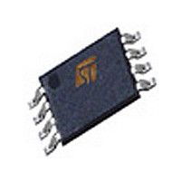
M93C66-WDW6T STMicroelectronics, M93C66-WDW6T Datasheet - Page 15

M93C66-WDW6T
Manufacturer Part Number
M93C66-WDW6T
Description
Manufacturer
STMicroelectronics
Datasheet
1.M93C66-WDW6T.pdf
(37 pages)
Specifications of M93C66-WDW6T
Density
4Kb
Interface Type
Serial (Microwire)
Organization
512x8/256x16
Frequency (max)
2MHz
Write Protection
No
Data Retention
40Year
Operating Supply Voltage (typ)
3.3/5V
Package Type
TSSOP
Operating Temp Range
-40C to 85C
Supply Current
2mA
Operating Supply Voltage (min)
2.5V
Operating Supply Voltage (max)
5.5V
Operating Temperature Classification
Industrial
Mounting
Surface Mount
Pin Count
8
Lead Free Status / Rohs Status
Not Compliant
Available stocks
Company
Part Number
Manufacturer
Quantity
Price
Company:
Part Number:
M93C66-WDW6T
Manufacturer:
ST
Quantity:
3 165
Part Number:
M93C66-WDW6TP
Manufacturer:
ST
Quantity:
20 000
M93C86, M93C76, M93C66, M93C56, M93C46
5.3
Figure 4.
1. For the meanings of An, Xn, Qn and Dn, see
Erase Byte or Word
The Erase Byte or Word (ERASE) instruction sets the bits of the addressed memory byte (or
word) to 1. Once the address has been correctly decoded, the falling edge of the Chip
Select Input (S) starts the self-timed Erase cycle. The completion of the cycle can be
detected by monitoring the READY/BUSY line, as described in the
section.
Read
Write
Write
Enable
READ, WRITE, WEN, WDS sequences
S
Q
S
S
Q
D
D
D
1 0
1
1 1 0 An
CODE
CODE
CODE
OP
OP
0
OP
1
0
1
An
1
ADDR
ADDR
Xn X0
A0
A0
Qn
Dn
Table
5.,
DATA OUT
DATA IN
Table 6.
Write
Disable
and
Table
S
D
D0
Q0
7..
BUSY
READY/BUSY status
1
CODE
STATUS
CHECK
0
OP
0
0
0
READY
Xn X0
Instructions
AI00878d
15/37


