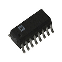
AD8803AR-REEL Analog Devices Inc, AD8803AR-REEL Datasheet - Page 4

AD8803AR-REEL
Manufacturer Part Number
AD8803AR-REEL
Description
Manufacturer
Analog Devices Inc
Datasheet
1.AD8803AR-REEL.pdf
(16 pages)
Specifications of AD8803AR-REEL
Number Of Channels
8
Resolution
8b
Conversion Rate
1.7MSPS
Interface Type
Serial (3-Wire/SPI)
Single Supply Voltage (typ)
3/5V
Dual Supply Voltage (typ)
Not RequiredV
Settling Time
0.6us
Architecture
R-2R
Power Supply Requirement
Single
Output Type
Voltage
Integral Nonlinearity Error
±1.5LSB
Single Supply Voltage (min)
2.7V
Single Supply Voltage (max)
5.5V
Dual Supply Voltage (min)
Not RequiredV
Dual Supply Voltage (max)
Not RequiredV
Operating Temp Range
-40C to 85C
Operating Temperature Classification
Industrial
Mounting
Surface Mount
Pin Count
16
Package Type
SOIC N
Lead Free Status / Rohs Status
Not Compliant
AD8801/AD8803
ADDR
B10 B9
A2
MSB
2
OPERATION
The AD8801/AD8803 provides eight channels of programmable
voltage output adjustment capability. Changing the programmed
output voltage of each TrimDAC is accomplished by clocking in
an 11-bit serial data word into the SDI (Serial Data Input) pin.
The format of this data word is three address bits, MSB first,
followed by eight data bits, MSB first. Table I provides the se-
rial register data word format. The AD8801/AD8803 has the
10
V
(DATA
V
DETAIL SERIAL DATA INPUT TIMING (RS = "1")
CLK
CLK
SDI
OUT
OUT
OCTAL 8-BIT TRIMDAC, WITH SHUTDOWN
CS
CS
SDI
IN)
A1
2
9
+5V
+5V
0V
0V
1
0
1
0
1
0
1
0
1
0
1
0
RESET TIMING
V
OUT
B8
A0
LSB MSB
2
RS
8
Figure 2b. Detail Timing Diagram
A2 A1 A0 D7 D6 D5 D4 D3 D2 D1 D0
A
Figure 2c. Reset Timing Diagram
Table I. Serial-Data Word Format
X
2.5V
+5V
OR D
t
Figure 2a. Timing Diagram
CSS
1
0
DATA
B7
D7
2
7
X
t
CH
B6
D6
2
A
6
t
X
DS
1 LSB ERROR BAND
OR D
t
CL
B5
D5
2
DAC REGISTER LOAD
X
t
5
RS
t
DH
t
1 LSB ERROR BAND
CSH
t
S
B4
D4
2
4
B3
D3
2
t
3
CS1
t
S
t
CSW
1 LSB
B2
D2
2
2
1 LSB
B1
D1
2
1
LSB
B0
D0
2
0
–4–
following address assignments for the ADDR decode which de-
termines the location of DAC register receiving the serial regis-
ter data in bits B7 through B0:
DAC outputs can be changed one at a time in random se-
quence. The fast serial-data loading of 33 MHz makes it possible
to load all eight DACs in as little time as 3 s (12
The exact timing requirements are shown in Figure 2.
The AD8801 offers a midscale preset activated by the RS pin
simplifying initial setting conditions at first power up. The
AD8803 has both a V
dent positive full-scale and zero-scale settings to optimize reso-
lution. Both parts offer a power shutdown SHDN that places
the DAC structure in a zero power consumption state resulting
in only leakage currents being consumed from the power supply,
V
latch settings are maintained. When returning to operational
mode from power shutdown the DAC outputs return to their
previous voltage settings.
PROGRAMMING THE OUTPUT VOLTAGE
The output voltage range is determined by the external refer-
ence connected to V
simplified diagram of the equivalent DAC circuit. In the case of
the AD8801, its V
therefore cannot be offset. V
can be tied to GND establishing a basic rail-to-rail voltage out-
put programming range. Other output ranges are established by
the use of different external voltage references. The general
transfer equation that determines the programmed output
voltage is:
where Dx is the data contained in the 8-bit DACx latch.
REF
Figure 3. AD8801/AD8803 Equivalent TrimDAC Circuit
inputs, and all 8 outputs. In shutdown mode the DACx
V
REGISTER
V
V
REFH
GND
REFL
O
DAC
(Dx) = (Dx)/256
D7
D6
D0
TO OTHER DACS
DAC # = A2
. .
.
REFL
P CH
N CH
. .
.
REFH
REFH
is internally connected to GND and
and V
and a V
REFH
(V
4 + A1
REFL
REFH
MSB
can be tied to V
REFL
pins. See Figure 3 for a
– V
LSB
2 + A0 + 1
pin to establish indepen-
REFL
) + V
2R
2R
2R
2R
DD
REFL
8
and V
. .
.
R
R
30 ns).
REV. A
O
X
REFL
(1)


