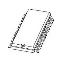
HEF4067BT NXP Semiconductors, HEF4067BT Datasheet - Page 12

HEF4067BT
Manufacturer Part Number
HEF4067BT
Description
Manufacturer
NXP Semiconductors
Type
Analog Multiplexerr
Datasheet
1.HEF4067BT.pdf
(19 pages)
Specifications of HEF4067BT
Multiplexer Configuration
Single 16:1
Number Of Inputs
16
Number Of Outputs
1
Number Of Channels
1
Analog Switch On Resistance
2500@5VOhm
Package Type
SO
Power Supply Requirement
Single
Single Supply Voltage (min)
3V
Single Supply Voltage (typ)
5/9/12V
Single Supply Voltage (max)
15V
Dual Supply Voltage (min)
Not RequiredV
Dual Supply Voltage (typ)
Not RequiredV
Dual Supply Voltage (max)
Not RequiredV
Supply Current
0.02@5VmA
Mounting
Surface Mount
Pin Count
24
Operating Temp Range
-40C to 85C
Operating Temperature Classification
Industrial
Lead Free Status / Rohs Status
Compliant
Available stocks
Company
Part Number
Manufacturer
Quantity
Price
Company:
Part Number:
HEF4067BT
Manufacturer:
RENESAS
Quantity:
340
NXP Semiconductors
Table 11.
V
[1]
Table 12.
P
HEF4067B_5
Product data sheet
Symbol
THD
f
α
V
Xtalk
Symbol
P
(−3dB)
SS
D
Fig 13. Test circuit for measuring total harmonic
iso
ct
D
can be calculated from the formulas shown; V
= 0 V; T
f
i
is biased at 0.5 V
V
DD
distortion
Additional dynamic characteristics
Dynamic power dissipation P
Parameter
dynamic power
dissipation
amb
or V
V
11.2.1 Test circuits
Parameter
total harmonic distortion
−3 dB frequency response
isolation (OFF-state)
crosstalk voltage
crosstalk
SS
SS
= 25
11.2 Additional dynamic parameters
°
DD
C.
A0 to A3
Z
fi
; V
I
E
= 0.5V
V
DD
V
5 V
10 V
15 V
DD
DD
V
Yn
SS
(p-p).
R L
All information provided in this document is subject to legal disclaimers.
Typical formula for P
P
P
P
D
Conditions
see
channel ON; V
f
see
channel ON; V
see
C
V
digital inputs to switch; see
R
E or An = V
between switches; see
f
V
D
D
D
i
i
001aag129
I
I
= 1 kHz
L
L
= 1 MHz; R
= 1000 × f
= 5500 × f
= 15000 × f
C L
= 0.5V
= 0.5V
= 5 pF; channel OFF;
= 10 kΩ; C
Figure
Figure
Figure
SS
D
Rev. 05 — 25 March 2010
= 0 V; t
DD
DD
13; R
14; R
15; f
DD
i
i
(p-p)
(p-p)
L
+ Σ(f
+ Σ(f
i
L
+ Σ(f
= 1 kΩ;
I
I
(square-wave)
r
= 15 pF;
= 0.5V
= 0.5V
i
= t
L
L
= 1 MHz; R
o
o
= 10 kΩ; C
= 1 kΩ; C
f
o
× C
× C
Fig 14. Test circuit for measuring frequency response
≤
× C
D
20 ns; T
DD
DD
(μW)
L
L
Figure
) × V
) × V
L
) × V
(p-p);
(p-p)
16-channel analog multiplexer/demultiplexer
V
Figure
L
L
DD
DD
DD
L
= 5 pF;
amb
= 1 kΩ;
DD
= 15 pF;
17;
or V
2
2
2
V
= 25
SS
SS
16;
°
C.
V
5 V
10 V
15 V
5 V
10 V
15 V
10 V
10 V
10 V
where:
f
f
C
V
Σ(C
A0 to A3
Z
fi
i
o
DD
DD
= input frequency in MHz;
L
= output frequency in MHz;
E
= output load capacitance in pF;
L
= supply voltage in V;
V
× f
DD
o
) = sum of the outputs.
V
[1]
[1]
[1]
[1]
[1]
[1]
[1]
[1]
Yn
SS
HEF4067B
Typ
0.25
0.04
0.04
13
40
70
−50
50
−50
R L
© NXP B.V. 2010. All rights reserved.
001aag235
Max
-
-
-
-
-
-
-
C L
-
-
dB
12 of 19
Unit
%
%
%
MHz
MHz
MHz
dB
mV
dB


