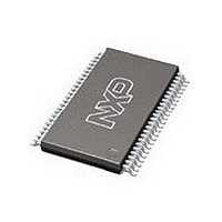
74LVC16244ADGG NXP Semiconductors, 74LVC16244ADGG Datasheet - Page 8

74LVC16244ADGG
Manufacturer Part Number
74LVC16244ADGG
Description
Manufacturer
NXP Semiconductors
Datasheet
1.74LVC16244ADGG.pdf
(19 pages)
Specifications of 74LVC16244ADGG
Logic Family
LVC
Logical Function
Buffer/Line Driver
Number Of Elements
4
Number Of Channels
16
Number Of Inputs
16
Number Of Outputs
16
Operating Supply Voltage (typ)
1.8/2.5/3.3V
Package Type
TSSOP
Output Type
3-State
Polarity
Non-Inverting
Propagation Delay Time
8ns
High Level Output Current
-24mA
Low Level Output Current
24mA
Operating Supply Voltage (max)
3.6V
Operating Supply Voltage (min)
1.2V
Quiescent Current
80uA
Technology
CMOS
Pin Count
48
Mounting
Surface Mount
Operating Temp Range
-40C to 125C
Operating Temperature Classification
Automotive
Lead Free Status / Rohs Status
Compliant
Available stocks
Company
Part Number
Manufacturer
Quantity
Price
Company:
Part Number:
74LVC16244ADGG
Manufacturer:
NXP
Quantity:
2 270
Part Number:
74LVC16244ADGG
Manufacturer:
NXP/恩智浦
Quantity:
20 000
Part Number:
74LVC16244ADGGR
Manufacturer:
PHILIPS/飞利浦
Quantity:
20 000
Company:
Part Number:
74LVC16244ADGGRG4
Manufacturer:
NXP
Quantity:
1 700
Company:
Part Number:
74LVC16244ADGGЈ¬118
Manufacturer:
NXP
Quantity:
2 000
NXP Semiconductors
Table 6.
At recommended operating conditions. Voltages are referenced to GND (ground = 0 V).
[1]
[2]
[3]
[4]
[5]
[6]
10. Dynamic characteristics
Table 7.
Voltages are referenced to GND (ground = 0 V). For test circuit see
74LVC_LVCH16244A_9
Product data sheet
Symbol Parameter
I
Symbol Parameter
t
t
t
BHHO
pd
en
dis
All typical values are measured at V
The bus hold circuit is switched off when V
For I/O ports the parameter I
Valid for data inputs of bus hold parts only (74LVCH16244A). Note that control inputs do not have a bus hold circuit.
The specified sustaining current at the data input holds the input below the specified V
The specified overdrive current at the data input forces the data input to the opposite input state.
propagation
delay
enable time
disable time
bus hold HIGH
overdrive current
Static characteristics
Dynamic characteristics
Conditions
nAn to nYn; see
nOE to nYn; see
nOE to nYn; see
V
V
V
V
V
V
V
V
V
OZ
CC
CC
CC
CC
CC
CC
CC
CC
CC
Conditions
V
CC
includes the input leakage current.
= 1.2 V
= 2.7 V
= 3.0 V to 3.6 V
= 1.2 V
= 2.7 V
= 3.0 V to 3.6 V
= 1.2 V
= 2.7 V
= 3.0 V to 3.6 V
= 3.6 V
…continued
CC
= 3.3 V (unless stated otherwise) and T
I
All information provided in this document is subject to legal disclaimers.
Figure 7
> V
Figure 8
Figure 8
CC
allowing 5.5 V on the input terminal.
Rev. 09 — 18 March 2010
74LVC16244A; 74LVCH16244A
16-bit buffer/line driver; 5 V input/output tolerant; 3-state
[4][6]
Figure
[1]
[2]
[1]
[2]
[1]
[2]
−500
Min
Min
−40 °C to +85 °C
1.0
1.1
1.0
1.0
1.0
1.8
amb
9.
-
-
-
−40 °C to +85 °C
= 25 °C.
I
Typ
level.
11.0
15.0
10.0
Typ
3.0
3.5
3.7
-
-
-
-
[1]
Max
Max
4.7
4.1
5.8
4.6
6.2
5.2
-
-
-
-
−40 °C to +125 °C Unit
−40 °C to +125 °C Unit
Min
−500
1.0
1.1
1.0
1.0
1.0
1.8
Min
-
-
-
© NXP B.V. 2010. All rights reserved.
Max
Max
6.0
5.5
7.5
6.0
8.0
6.5
-
-
-
-
μA
8 of 19
ns
ns
ns
ns
ns
ns
ns
ns
ns


