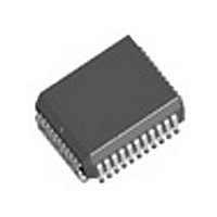
TXC02050AIPL Transwitch Corporation, TXC02050AIPL Datasheet - Page 3

TXC02050AIPL
Manufacturer Part Number
TXC02050AIPL
Description
Manufacturer
Transwitch Corporation
Datasheet
1.TXC02050AIPL.pdf
(26 pages)
Specifications of TXC02050AIPL
Operating Temperature (min)
-40C
Operating Temperature Classification
Industrial
Operating Temperature (max)
85C
Package Type
PLCC
Rad Hardened
No
Lead Free Status / Rohs Status
Not Compliant
Two Terminal Side interfaces are provided, a positive and negative rail (RP and RN) or NRZ (RD) interface.
The selection is determined by the state placed on the signal lead labeled PNENB. When a low is applied to
the signal lead, the HDB3 Decoder and HDB3 Encoder Blocks are bypassed, and the terminal side I/O is a
positive and negative rail interface. When a high is applied to the signal lead, an NRZ interface is provided.
Data is clocked out of the MRT on negative edges of the clock signal (CLKO). Receive data and the clock sig-
nals are disabled, and forced to a high impedance state by placing a low on the receive disable lead (RXDIS).
For a receive positive and negative rail interface, an inverted clock (CLKO) is also provided.
The terminal side interface for the transmitter can either be positive and negative rail (TP and TN) or NRZ (TD)
data depending on the state of the common control lead PNENB. Data is clocked into the MRT on positive
transitions of the clock signal (CLKI). The input clock is monitored for the loss of clock. When the input clock
remains high or low, TXLOC will be set low. The MRT also provides the capability to generate and insert AIS
(all ones signal), independent of the transmit data. A low placed on the TXAIS lead enables the transmit AIS
generator.
Two loopbacks are provided, transmit loopback and receive loopback. Transmit loopback connects the data
path from the transmitter output driver stage to the clock recovery, and disables the external receiver input.
Transmit loopback is activated by placing a low on the LBKTX signal lead.
Receive loopback connects the receive data path to the transmit output circuits and disables the transmit input.
Receive loopback is activated by placing a low on the LBKRX signal lead.
For 6 Mbps operation, the MRT should be operated in the P and N rail mode, bypassing the HDB3 Decoder/
Encoder.
PIN DIAGRAM
Figure 2. MRT Pin Diagram With Names and Numbers
PNENB
RP/RD
VCOC
CLKO
CLKO
PLLC
GND
GND
DCK
VDD
RN
8
10
12
14
16
MRT PIN DIAGRAM
- 3 -
(Top View)
38
36
34
32
30
GND
CLKI
VDD
GND
VDD
TPO
TNO
GND
GNDA
DI2
DI1
Ed. 3, April 1994
TXC-02050-MB
MRT


