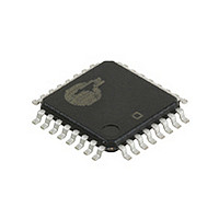
CY29940AC-1 Cypress Semiconductor Corp, CY29940AC-1 Datasheet - Page 3

CY29940AC-1
Manufacturer Part Number
CY29940AC-1
Description
Manufacturer
Cypress Semiconductor Corp
Type
Clock Driverr
Datasheet
1.CY29940AC-1.pdf
(7 pages)
Specifications of CY29940AC-1
Number Of Clock Inputs
2
Output Frequency
200MHz
Output Logic Level
LVCMOS/LVTTL
Operating Supply Voltage (min)
2.375V
Operating Supply Voltage (typ)
2.5/3.3V
Operating Supply Voltage (max)
3.465V
Package Type
TQFP
Operating Temp Range
0C to 70C
Operating Temperature Classification
Commercial
Signal Type
LVCMOS/LVPECL/LVTTL
Mounting
Surface Mount
Pin Count
32
Quiescent Current
7mA
Lead Free Status / Rohs Status
Not Compliant
Available stocks
Company
Part Number
Manufacturer
Quantity
Price
Company:
Part Number:
CY29940AC-1
Manufacturer:
CY
Quantity:
2 147
Document #: 38-07487 Rev. **
Absolute Maximum Conditions
Maximum Input Voltage Relative to V
Maximum Input Voltage Relative to V
Storage Temperature: ................................–65 C to + 150 C
Operating Temperature: ................................ –40 C to +85 C
Maximum ESD Protection............................................... 2 kV
Maximum Power Supply: ................................................5.5V
Maximum Input Current: ............................................±20 mA
DC Electrical Specifications:
Notes:
2.
3.
4.
5.
6.
V
V
I
I
V
V
V
V
I
I
Z
C
IL
IH
DDQ
DD
Parameter
IL
IH
PP
CMR
OL
OH
out
in
Inputs have pull-up/pull-down resistors that effect input current.
The VCMR is the difference from the most positive side of the differential input signal. Normal operation is obtained when the “High” input is within the VCMR
range and the input lies within the VPP specification. Driving series or parallel terminated 50
Outputs driving 50 transmission lines.
See Figure 1 and Figure 2.
50% input duty cycle.
Input Low Voltage
Input High Voltage
Input Low Current
Input High Current
Peak-to-Peak Input Voltage
PECL_CLK
Common Mode Range
PECL_CLK
Output Low Voltage
Output High Voltage
Quiescent Supply Current
Dynamic Supply Current
Output Impedance
Input Capacitance
Description
[2]
[2]
[4,5,6]
SS
DD
[4,5,6]
V
: ............ V
: ............. V
DD
[3]
= 3.3V ±5% or 2.5V ±5%, V
DD
SS
– 0.3V
+ 0.3V
V
V
I
I
I
I
V
150 MHz, CL=10 pF
V
200 MHz, CL=10 pF
V
150 MHz, CL=10 pF
V
200 MHz, CL=10 pF
OL
OL
OH
OH
DD
DD
DD
DD
DD
DD
= 20 mA, V
= 16 mA, V
= –20 mA, V
= –16 mA, V
= 3.3V
= 2.5V
= 3.3V, Outputs @
= 3.3V, Outputs @
= 2.5V, Outputs @
= 2.5V, Outputs @
This device contains circuitry to protect the inputs against
damage due to high static voltages or electric field; however,
precautions should be taken to avoid application of any
voltage higher than the maximum rated voltages to this circuit.
For proper operation, V
range:
V
Unused inputs must always be tied to an appropriate logic
voltage level (either V
Conditions
SS
< (V
DDC
DDC
DDC
in
DDC
DDC
= 3.3V ±5% or 2.5V ±5%
or V
(or 50
= 3.3V
= 2.5V
= 3.3V
= 2.5V
out
) < V
to VDD/2) transmission lines.
SS
DD
V
V
in
DD
DD
and V
or V
Min.
V
500
2.0
2.4
1.8
18
SS
– 1.4
– 1.0
DD
out
).
should be constrained to the
Typ.
285
335
200
240
23
5
4
V
V
CY29940-1
DD
DD
Max.
–200
1000
V
200
0.8
0.5
28
7
DD
– 0.6
– 0.6
Page 3 of 7
Unit
mV
mA
mA
µA
µA
pF
V
V
V
V
V
[+] Feedback


