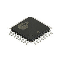
CY29940AC-1 Cypress Semiconductor Corp, CY29940AC-1 Datasheet

CY29940AC-1
Specifications of CY29940AC-1
Available stocks
Related parts for CY29940AC-1
CY29940AC-1 Summary of contents
Page 1
... Block Diagram VDD PECL_CLK 0 PECL_CLK# 1 TCLK TCLK_SEL Cypress Semiconductor Corporation Document #: 38-07487 Rev. ** 2.5V or 3.3V, 200-MHz 1:18 Clock Distribution Buffer Description The CY29940 low-voltage 200-MHz clock distribution buffer with the capability to select either a differential LVPECL LVCMOS/LVTTL-compatible input clock. The two clock ...
Page 2
Pin Description Pin Name PWR 5 PECL_CLK 6 PECL_CLK# 3 TCLK 9, 10, 11, 13, Q(17:0) VDDC 14, 15, 18, 19, 20, 22, 23, 24, 26, 27, 28, 30, 31 TCLK_SEL 8, 16, 29 VDDC 7, 21 ...
Page 3
Absolute Maximum Conditions Maximum Input Voltage Relative ............ V SS Maximum Input Voltage Relative ............. V DD Storage Temperature: ................................– 150 C Operating Temperature: ................................ – +85 C Maximum ...
Page 4
AC Electrical Specifications (V DD Parameter Description F Input Frequency max [4,5,10] T PECL_CLK to Q Delay PD </ =150 MHz [4,5,10] LVCMOS to Q Delay </ =150 MHz [4,5,6] FoutDC Output Duty Cycle [4,5] T Output-to-Output Skew skew [8] ...
Page 5
... LVCMOS_CLK Figure 4. LVCMOS Propagation Delay (TPD) Test Reference Ordering Information Part Number CY29940AC–1 32-pin TQFP CY29940AC–1T 32-pin TQFP – Tape and Reel CY29940AI–1 32-pin TQFP CY29940AI–1T 32-pin TQFP – Tape and Reel Document #: 38-07487 Rev CMR VCC ...
Page 6
... Document #: 38-07487 Rev. ** © Cypress Semiconductor Corporation, 2003. The information contained herein is subject to change without notice. Cypress Semiconductor Corporation assumes no responsibility for the use of any circuitry other than circuitry embodied in a Cypress Semiconductor product. Nor does it convey or imply any license under patent or other rights. Cypress Semiconductor does not authorize its products for use as critical components in life-support systems where a malfunction or failure may reasonably be expected to result in significant injury to the user ...
Page 7
Document History Page Document Title: CY29940-1 2.5V or 3.3V, 200-MHz 1:18 Clock Distribution Buffer Document Number: 38-07487 Issue REV. ECN NO. Date ** 119820 01/29/03 Document #: 38-07487 Rev. ** Orig. of Change Description of Change BRK New Data Sheet ...


