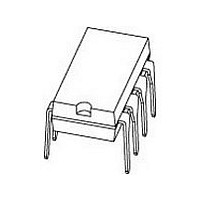
TDA7052A NXP Semiconductors, TDA7052A Datasheet - Page 4

TDA7052A
Manufacturer Part Number
TDA7052A
Description
Manufacturer
NXP Semiconductors
Datasheet
1.TDA7052A.pdf
(14 pages)
Specifications of TDA7052A
Operational Class
Class-AB
Audio Amplifier Output Configuration
1-Channel Mono
Output Power (typ)
1.1x1@8OhmW
Audio Amplifier Function
Speaker
Total Harmonic Distortion
0.3@8Ohm@500mW%
Single Supply Voltage (typ)
5/9/12/15V
Dual Supply Voltage (typ)
Not RequiredV
Power Supply Requirement
Single
Power Dissipation
1.25W
Rail/rail I/o Type
No
Power Supply Rejection Ratio
46dB
Single Supply Voltage (min)
4.5V
Single Supply Voltage (max)
18V
Dual Supply Voltage (min)
Not RequiredV
Dual Supply Voltage (max)
Not RequiredV
Operating Temp Range
-40C to 85C
Operating Temperature Classification
Industrial
Mounting
Through Hole
Pin Count
8
Package Type
PDIP
Lead Free Status / Rohs Status
Compliant
Available stocks
Company
Part Number
Manufacturer
Quantity
Price
Company:
Part Number:
TDA7052A
Manufacturer:
PHILIPS
Quantity:
654
Company:
Part Number:
TDA7052A
Manufacturer:
NXPL
Quantity:
4 770
Company:
Part Number:
TDA7052A
Manufacturer:
TOS
Quantity:
4 780
Part Number:
TDA7052A
Manufacturer:
PHILIPS/飞利浦
Quantity:
20 000
Company:
Part Number:
TDA7052A/B
Manufacturer:
HARR
Quantity:
68
Part Number:
TDA7052A/N2,112
Manufacturer:
NXP/恩智浦
Quantity:
20 000
Company:
Part Number:
TDA7052AT
Manufacturer:
AMD
Quantity:
6 218
Part Number:
TDA7052AT
Manufacturer:
PHILIPS/飞利浦
Quantity:
20 000
Part Number:
TDA7052AT/N2
Manufacturer:
NXP/恩智浦
Quantity:
20 000
NXP Semiconductors
FUNCTIONAL DESCRIPTION
The TDA7052A/AT are mono BTL output amplifiers with
DC volume control, designed for use in TV and monitors
but also suitable for battery fed portable recorders and
radios.
In conventional DC volume circuits the control or input
stage is AC coupled to the output stage via external
capacitors to keep the offset voltage low.
In the TDA7052A/AT the DC volume control stage is
integrated into the input stage so that no coupling
capacitors are required and yet a low offset voltage is
maintained. At the same time the minimum supply remains
low.
The BTL principle offers the following advantages:
• Lower peak value of the supply current
• The frequency of the ripple on the supply voltage is twice
LIMITING VALUES
In accordance with the Absolute Maximum System (IEC 134)
July 1994
V
I
I
P
T
T
T
T
V
V
ORM
OSM
the signal frequency.
amb
stg
vj
sc
P
tot
2
4
1 W BTL mono audio amplifier with DC
volume control
SYMBOL
supply voltage range
repetitive peak output current
non-repetitive peak output current
total power dissipation
operating ambient temperature range
storage temperature range
virtual junction temperature
short-circuit time
input voltage pin 2
input voltage pin 4
TDA7052A
TDA7052AT
PARAMETER
4
Thus a reduced power supply with smaller capacitors can
be used which results in cost savings.
For portable applications there is a trend to decrease the
supply voltage, resulting in a reduction of output power at
conventional output stages. Using the BTL principle
increases the output power.
The maximum gain of the amplifier is fixed at 35.5 dB. The
DC volume control stage has a logarithmic control
characteristic.
The total gain can be controlled from 35.5 dB to −44 dB. If
the DC volume control voltage is below 0.3 V, the device
switches to the mute mode.
The amplifier is short-circuit proof to ground, V
across the load. Also a thermal protection circuit is
implemented. If the crystal temperature rises above
+150 °C the gain will be reduced, so the output power is
reduced.
Special attention is given to switch on and off clicks, low
HF radiation and a good overall stability.
T
amb
CONDITIONS
≤ 25%
−
−
−
−
−
−40
−55
−
−
−
−
MIN.
TDA7052A/AT
18
1.25
1.5
1.25
0.8
+85
+150
+150
1
8
8
Product specification
MAX.
P
V
A
A
W
W
°C
°C
°C
hr
V
V
and
UNIT


