TDA1517P NXP Semiconductors, TDA1517P Datasheet - Page 4
TDA1517P
Manufacturer Part Number
TDA1517P
Description
Manufacturer
NXP Semiconductors
Datasheet
1.TDA1517P.pdf
(15 pages)
Specifications of TDA1517P
Operational Class
Class-B
Audio Amplifier Output Configuration
2-Channel Stereo
Output Power (typ)
6x2@4OhmW
Audio Amplifier Function
Speaker
Total Harmonic Distortion
0.1@4Ohm@1W%
Single Supply Voltage (typ)
14.4V
Dual Supply Voltage (typ)
Not RequiredV
Power Supply Requirement
Single
Power Dissipation
15W
Rail/rail I/o Type
No
Power Supply Rejection Ratio
80dB
Single Supply Voltage (min)
6V
Single Supply Voltage (max)
18V
Dual Supply Voltage (min)
Not RequiredV
Dual Supply Voltage (max)
Not RequiredV
Operating Temp Range
-40C to 85C
Operating Temperature Classification
Industrial
Mounting
Through Hole
Pin Count
18
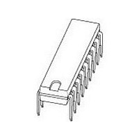
Package Type
HDIP
Lead Free Status / Rohs Status
Compliant
Available stocks
Company
Part Number
Manufacturer
Quantity
Price
Company:

Part Number:
TDA1517P
Manufacturer:
PHILIPS
Quantity:
505
Part Number:
TDA1517P
Manufacturer:
NXP/恩智浦
Quantity:
20 000
Company:
Part Number:
TDA1517P/N3
Manufacturer:
NXP Semiconductors
Quantity:
1 966
Company:
Part Number:
TDA1517P/N3
Manufacturer:
NXP
Quantity:
20 000
Company:
Part Number:
TDA1517PN3
Manufacturer:
ON
Quantity:
7 272


NXP Semiconductors
PINNING
FUNCTIONAL DESCRIPTION
The TDA1517 contains two identical amplifiers with
differential input stages. The gain of each amplifier is fixed
at 20 dB. A special feature of the device is the
mute/standby switch which has the following features:
• Low standby current (<100 μA)
• Low mute/standby switching current
• Mute condition.
2004 Feb 18
handbook, halfpage
−INV1
SGND
SVRR
OUT1
PGND
OUT2
V
M/SS
−INV2
(low cost supply switch)
P
2 x 6 W stereo power amplifier
Fig.2
SYMBOL
Pin configuration for SOT110-1 and
SOT352-1.
SGND
PGND
SVRR
OUT1
OUT2
M/SS
INV1
INV2
V
P
3
4
1
2
5
6
7
8
9
TDA1517
MLC352
PIN
1
2
3
4
5
6
7
8
9
non-inverting input 1
signal ground
supply voltage ripple rejection output
output 1
power ground
output 2
supply voltage
mute/standby switch input
non-inverting input 2
4
handbook, halfpage
Pins 10 to 18 should be connected to GND or floating.
Fig.3 Pin configuration for SOT398-1.
DESCRIPTION
SGND
PGND
SVRR
OUT1
OUT2
M/SS
INV1
INV2
V
P
TDA1517; TDA1517P
3
4
1
2
5
6
7
8
9
TDA1517P
MLC353
Product specification
16
15
18
17
14
13
12
11
10
Related parts for TDA1517P
Image
Part Number
Description
Manufacturer
Datasheet
Request
R

Part Number:
Description:
NXP Semiconductors designed the LPC2420/2460 microcontroller around a 16-bit/32-bitARM7TDMI-S CPU core with real-time debug interfaces that include both JTAG andembedded trace
Manufacturer:
NXP Semiconductors
Datasheet:

Part Number:
Description:
NXP Semiconductors designed the LPC2458 microcontroller around a 16-bit/32-bitARM7TDMI-S CPU core with real-time debug interfaces that include both JTAG andembedded trace
Manufacturer:
NXP Semiconductors
Datasheet:
Part Number:
Description:
NXP Semiconductors designed the LPC2468 microcontroller around a 16-bit/32-bitARM7TDMI-S CPU core with real-time debug interfaces that include both JTAG andembedded trace
Manufacturer:
NXP Semiconductors
Datasheet:
Part Number:
Description:
NXP Semiconductors designed the LPC2470 microcontroller, powered by theARM7TDMI-S core, to be a highly integrated microcontroller for a wide range ofapplications that require advanced communications and high quality graphic displays
Manufacturer:
NXP Semiconductors
Datasheet:
Part Number:
Description:
NXP Semiconductors designed the LPC2478 microcontroller, powered by theARM7TDMI-S core, to be a highly integrated microcontroller for a wide range ofapplications that require advanced communications and high quality graphic displays
Manufacturer:
NXP Semiconductors
Datasheet:
Part Number:
Description:
The Philips Semiconductors XA (eXtended Architecture) family of 16-bit single-chip microcontrollers is powerful enough to easily handle the requirements of high performance embedded applications, yet inexpensive enough to compete in the market for hi
Manufacturer:
NXP Semiconductors
Datasheet:
Part Number:
Description:
The XA-S3 device is a member of Philips Semiconductors? XA(eXtended Architecture) family of high performance 16-bitsingle-chip microcontrollers
Manufacturer:
NXP Semiconductors
Datasheet:

Part Number:
Description:
The NXP BlueStreak LH75401/LH75411 family consists of two low-cost 16/32-bit System-on-Chip (SoC) devices
Manufacturer:
NXP Semiconductors
Datasheet:
Part Number:
Description:
The NXP LPC3130/3131 combine an 180 MHz ARM926EJ-S CPU core, high-speed USB2
Manufacturer:
NXP Semiconductors
Datasheet:
Part Number:
Description:
The NXP LPC3141 combine a 270 MHz ARM926EJ-S CPU core, High-speed USB 2
Manufacturer:
NXP Semiconductors
Part Number:
Description:
The NXP LPC3143 combine a 270 MHz ARM926EJ-S CPU core, High-speed USB 2
Manufacturer:
NXP Semiconductors

Part Number:
Description:
The NXP LPC3152 combines an 180 MHz ARM926EJ-S CPU core, High-speed USB 2
Manufacturer:
NXP Semiconductors
Part Number:
Description:
The NXP LPC3154 combines an 180 MHz ARM926EJ-S CPU core, High-speed USB 2
Manufacturer:
NXP Semiconductors

Part Number:
Description:
Standard level N-channel enhancement mode Field-Effect Transistor (FET) in a plastic package using NXP High-Performance Automotive (HPA) TrenchMOS technology
Manufacturer:
NXP Semiconductors
Datasheet: