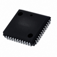
HA456CMZ Intersil, HA456CMZ Datasheet - Page 6

HA456CMZ
Manufacturer Part Number
HA456CMZ
Description
IC SWITCH CROSS VIDEO 8X8 44PLCC
Manufacturer
Intersil
Datasheet
1.HA456CMZ.pdf
(13 pages)
Specifications of HA456CMZ
Function
Video Crosspoint Switch
Circuit
1 x 8:1
Voltage Supply Source
Single Supply
Voltage - Supply, Single/dual (±)
4.5 V ~ 5.5 V
Current - Supply
68mA
Operating Temperature
0°C ~ 70°C
Mounting Type
Surface Mount
Package / Case
44-LCC (J-Lead)
Control Interface
Parallel, Serial
Supply Voltage Range
± 4.5V To ± 5.5V
Operating Temperature Range
0°C To +70°C
Digital Ic Case Style
PLCC
No. Of Pins
44
Termination Type
SMD
Rohs Compliant
Yes
Filter Terminals
SMD
Lead Free Status / RoHS Status
Lead free / RoHS Compliant
Available stocks
Company
Part Number
Manufacturer
Quantity
Price
Company:
Part Number:
HA456CMZ
Manufacturer:
ALTERA
Quantity:
51
Application Information
HA456 Architecture
The HA456 video crosspoint switch consists of 64 switches in
an 8x8 grid (see Figure 1). Each input is fully buffered and
presents a constant input capacitance whether the input
connects to one output or all 8 outputs. This yields consistent
input termination impedances regardless of the switch
configuration. The 8 matrix outputs are followed by 8 unity gain,
wideband, tristatable buffers optimized for driving 400Ω and
5pF loads. The output disable function is useful for multiplexing
two or more HA456s to create a larger input matrix (e.g., two
multiplexed HA456s yield a 16x8 crosspoint).
The HA456 outputs can be disabled individually or
collectively under software control. When disabled, an output
enters a high-impedance state. In multichip parallel
applications, the disable function prevents inactive outputs
from loading lines driven by other devices. Disabling an
unused output also reduces power consumption.
The HA456 outputs connect easily to two HFA1412 quad,
gain-of-two buffers when 75Ω loads must be driven.
Power-On RESET
The HA456 has an internal power-on reset (POR) circuit that
disables all outputs at power-up, and presets the switch
matrix so that all outputs connect to IN0. In parallel mode,
the desired switch state may be programmed before the
outputs are enabled. In serial mode, all outputs are
connected to GND each time they are enabled, so switch
state programming must occur after the output is enabled.
Digital Interface
The desired switch state can be loaded using a 7-bit parallel
interface mode or 32-bit serial interface mode (see Tables 1
through 3). All actions associated with the WR line occur on
its rising edge. The same is true for the LATCH line if
SELECT AND
COMMAND
CODES OR
SERIAL I/O
INPUTS
VIDEO
OUTPUT
SELECT
INPUT
WR
LATCH
A2
A1
A0
D3
D2
D1/SER OUT
D0/SER IN
BUFFERS
6
INPUT
FIGURE 1. TYPICAL CABLE DRIVING APPLICATION
HA456
SWITCH
MATRIX
8X8
HA456
EDGE/LEVEL = 1. Otherwise, the Slave Register updates
asynchronously (while LATCH=0, if EDGE/LEVEL = 0). WR
is logically AND’ed with CE and CE to allow active high or
active low chip enable.
7-Bit Parallel Mode
In the parallel programming mode (SER/PAR = 0), the 7 control
bits (A2:0 and D3:0) typically specify an output channel (A2:0)
and the corresponding action to be taken (D3:0). Command
codes are available to enable or disable all outputs, or
individual outputs, as shown in Table 1. Each output has 4-bit
Master and Slave Registers associated with it that hold the
output’s currently selected input address (defined by D3:0). The
input address (if applicable) is loaded into the Master Register
on the rising edge of WR. If the HA456 is in level mode, and if
LATCH = 0 (asynchronous switching), then the input address
flows through the transparent Slave Register and the output
immediately switches to the new input. For synchronous
switching on the rising edge of LATCH, strap the HA456 for
edge mode, program all the desired switch connections, and
then drive an inverted pulse on the LATCH input. Note:
Operations defined by commands 1011 - 1111 occur
asynchronously on the WR rising edge, without regard for the
state of LATCH or EDGE/LEVEL.
32-Bit Serial Mode
In the serial programming mode, all master registers are loaded
with data, making it unnecessary to specify an output address
(A2:0). The input data format is D3-D0, starting with OUT0 and
ending with OUT7 for 32 total bits (i.e., first bit shifted in is D3
for OUT0, and 32nd bit shifted in is D0 for OUT7). Only codes
0000 through 1010 are valid serial mode commands. Code
1010 disables an individual output, while code 1001 enables it.
After data is shifted into the 32-bit Master Register, it transfers
to the Slave Register on the rising edge of the LATCH line
(Edge mode), or when LATCH = 0 (Level mode, see Figure 5).
A
A
V
V
= +2
= +2
HFA1412 OR
HFA1405
75Ω
75Ω
September 26, 2008
VIDEO
OUT
FN4153.7


