HA456CMZ Intersil, HA456CMZ Datasheet
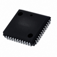
IC SWITCH CROSS VIDEO 8X8 44PLCC

HA456CMZ

Manufacturer Part Number
HA456CMZ
Description
IC SWITCH CROSS VIDEO 8X8 44PLCC
Manufacturer
Intersil
Datasheet

Specifications of HA456CMZ

Function
Video Crosspoint Switch
Circuit
1 x 8:1
Voltage Supply Source
Single Supply
Voltage - Supply, Single/dual (±)
4.5 V ~ 5.5 V
Current - Supply
68mA
Operating Temperature
0°C ~ 70°C
Mounting Type
Surface Mount
Package / Case
44-LCC (J-Lead)
Control Interface
Parallel, Serial
Supply Voltage Range
± 4.5V To ± 5.5V
Operating Temperature Range
0°C To +70°C
Digital Ic Case Style
PLCC
No. Of Pins
44
Termination Type
SMD
Rohs Compliant
Yes
Filter Terminals
SMD
Lead Free Status / RoHS Status
Lead free / RoHS Compliant

Available stocks

Company
Part Number
Manufacturer
Quantity
Price
Part Number:
HA456CMZ
Manufacturer:
ALTERA
Quantity:
51
Part Number:
HA456CMZ
Manufacturer:
INTERSI
Quantity:
2 486
Part Number:
HA456CMZ
Manufacturer:
Intersil
Quantity:
10 000
120MHz, Low Power, 8x8 Video
Crosspoint Switch
The HA456 is the first 8x8 video crosspoint switch suitable
for high performance video systems. Its high level of
integration significantly reduces component count, board
space, and cost. The crosspoint switch contains a digitally
controlled matrix of 64 fully buffered switches that connect 8
video input signals to any, or all, matrix outputs. Each matrix
output connects to an internal, high-speed (200V/µs), unity
gain buffer capable of driving 400Ω and 5pF to ±2V.
For applications requiring gain or increased drive capability,
the HA456 outputs can be connected directly to two
HFA1412 quad, gain of two video buffers, which are capable
of driving 75Ω loads.
This crosspoint’s true high impedance three-state output
capability, makes it feasible to parallel multiple HA456s and
form larger switch matrices.
Ordering Information
NOTE: These Intersil Pb-free plastic packaged products employ
special Pb-free material sets, molding compounds/die attach
materials, and 100% matte tin plate plus anneal (e3 termination
finish, which is RoHS compliant and compatible with both SnPb and
Pb-free soldering operations). Intersil Pb-free products are MSL
classified at Pb-free peak reflow temperatures that meet or exceed
the Pb-free requirements of IPC/JEDEC J STD-020.
HA456CM
HA456CMZ
(Note)
NUMBER
PART
HA456CM
HA456CMZ
MARKING
PART
RANGE
0 to +70 44 Ld PLCC
0 to +70 44 Ld PLCC
TEMP.
®
(°C)
1
(Pb-free)
Data Sheet
PACKAGE
N44.65
N44.65
DWG. #
PKG.
1-888-INTERSIL or 1-888-468-3774
CAUTION: These devices are sensitive to electrostatic discharge; follow proper IC Handling Procedures.
Features
• Fully Buffered Inputs and Outputs (A
• Routes Any Input Channel to Any Output Channel
• Switches Standard and High Resolution Video Signals
• Serial or Parallel Digital Interface
• Expandable for Larger Switch Matrices
• Wide Bandwidth . . . . . . . . . . . . . . . . . . . . . . . . . . 120MHz
• High Slew Rate . . . . . . . . . . . . . . . . . . . . . . . . . . 200V/µs
• Differential Gain and Phase . . . . . . . . . . . . . .0.05%, 0.05°
• Low Crosstalk at 10MHz . . . . . . . . . . . . . . . . . . . . . -55dB
• Pb-Free Available (RoHS Compliant)
Applications
• Professional Video Switching and Routing
• Security and Video Editing Systems
Pinout
September 26, 2008
EDGE/LEVEL
Copyright © Intersil Americas Inc. 2003, 2006, 2007, 2008. All Rights Reserved.
DGND
DGND
All other trademarks mentioned are the property of their respective owners.
IN1
IN2
IN3
IN4
IN5
NC
NC
A0
|
Intersil (and design) is a registered trademark of Intersil Americas Inc.
10
11
12
14
15
16
17
7
8
9
13
18
6
19
5
20
4
(44 LD PLCC)
21
TOP VIEW
3
HA456
22
2
23
1
44 43 42 41 40
24
25
26
V
27
= +1)
28
39
38
37
36
35
34
33
32
31
30
29
HA456
FN4153.7
OUT2
V-
OUT3
AGND
OUT4
NC
AGND
OUT5
AGND
OUT6
V+

Related parts for HA456CMZ

HA456CMZ Summary of contents

Page 1

... MARKING (°C) PACKAGE HA456CM HA456CM PLCC HA456CMZ HA456CMZ PLCC (Note) (Pb-free) NOTE: These Intersil Pb-free plastic packaged products employ special Pb-free material sets, molding compounds/die attach materials, and 100% matte tin plate plus anneal (e3 termination finish, which is RoHS compliant and compatible with both SnPb and Pb-free soldering operations) ...

Page 2

HA456 Functional Block Diagram IN0 IN1 IN2 SER/PAR D0/SER HA456 IN3 IN4 IN5 IN6 IN7 HA456 8x8 SWITCH MATRIX EN0:7 SLAVE REGISTER MASTER REGISTER OUTPUT BUFFERS ( OUT0 EN0 OUT7 ...

Page 3

Pin Descriptions NAME NC No connect. Not internally connected. D1/SER OUT Parallel Data Bit input D1 for Parallel Programming Mode. Serial Data Output (MSB of shift register) for cascading multiple HA456s in serial programming mode. Simply connect Serial Data Out ...

Page 4

... Thermal Information Thermal Resistance (Typical, Note 1) PLCC Package Maximum Junction Temperature . . . . . . . . . . . . . . . . . . . . . +150°C Maximum Storage Temperature Range . . . . . . . . . -65°C to +150°C Pb-free reflow profile . . . . . . . . . . . . . . . . . . . . . . . . . .see link below SUPPLY http://www.intersil.com/pbfree/Pb-FreeReflow.asp = 400Ω (Note 2), Unless Otherwise Specified. = ±5V, AGND = DGND = 0V LEVEL TEST CONDITIONS (Note ...

Page 5

Electrical Specifications V SUPPLY PARAMETER Output Capacitance (Output Disabled) Power Supply Rejection Ratio Digital Input Current (Note 5) Digital Input Low Voltage Digital Input High Voltage SER OUT Logic Low Voltage SER OUT Logic High Voltage AC CHARACTERISTICS (Note 4) ...

Page 6

Application Information HA456 Architecture The HA456 video crosspoint switch consists of 64 switches in an 8x8 grid (see Figure 1). Each input is fully buffered and presents a constant input capacitance whether the input connects to one output or all ...

Page 7

A2:0 D3:0 Selects 0000 to 0111 Connect the input defined by D3:0 to the output selected by A2:0. Doesn’t enable a disabled output. Output 1000 Connect the output selected by A2:0 to GND. Doesn’t enable a disabled output. Being Programmed ...

Page 8

IN0 8 IN1 10 IN2 13 IN3 VIDEO 15 INPUTS IN4 17 IN5 19 IN6 21 IN7 D0/SER D1/SER OUT ...

Page 9

Waveforms (Continued) WR LATCH MASTER REGISTER CONTENTS SLAVE REGISTER CONTENTS (EDGE/LEVEL = 0) SLAVE REGISTER CONTENTS (EDGE/LEVEL = 1) FIGURE 4. PARALLEL PROGRAMMING MODE OPERATION (SER/PAR = 0) D3 SER IN 1st WRITE WR LATCH SLAVE REGISTER ...

Page 10

AC Test Circuits IN0 OUT0 IN1 OUT1 OUT2 IN2 IN3 OUT3 IN4 OUT4 IN5 OUT5 IN6 OUT6 OUT7 IN7 SWEEP FREQUENCY IN P-P FIGURE 6. -3dB BANDWIDTH (NOTES 8 thru 11) IN0 OUT0 IN1 OUT1 OUT2 ...

Page 11

Typical Performance Curves 1.4 1.2 1.0 0.8 0.6 0.4 0.2 0 -0.2 TIME (20ns/DIV) FIGURE 10. SMALL SIGNAL PULSE RESPONSE 3 GAIN OUT P OUT P-P PHASE OUT ...

Page 12

Typical Performance Curves 250 225 200 175 150 125 100 75 50 0.5 1.0 1.5 2.0 2.5 3.0 3 OUT P-P FIGURE 16. SLEW RATE vs V FIGURE 18. FREQUENCY RESPONSE OF HA456-HFA1412 COMBINATION (PER FIGURE 2) 12 ...

Page 13

... Accordingly, the reader is cautioned to verify that data sheets are current before placing orders. Information furnished by Intersil is believed to be accurate and reliable. However, no responsibility is assumed by Intersil or its subsidiaries for its use; nor for any infringements of patents or other rights of third parties which may result from its use ...

Related keywords