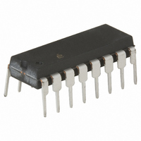
HI1-0539-5 Intersil, HI1-0539-5 Datasheet - Page 9

HI1-0539-5
Manufacturer Part Number
HI1-0539-5
Description
IC MULTIPLEXER 4X1 16CDIP
Manufacturer
Intersil
Datasheet
1.HI1-0539-5.pdf
(12 pages)
Specifications of HI1-0539-5
Function
Multiplexer
Circuit
1 x 4:1
On-state Resistance
850 Ohm
Voltage Supply Source
Dual Supply
Voltage - Supply, Single/dual (±)
±5 V ~ 18 V
Current - Supply
0.001mA
Operating Temperature
0°C ~ 75°C
Mounting Type
Through Hole
Package / Case
16-CDIP (0.300", 7.62mm)
Lead Free Status / RoHS Status
Contains lead / RoHS non-compliant
Available stocks
Company
Part Number
Manufacturer
Quantity
Price
Provide Path For I
The input bias current for any DC-coupled amplifier must
have an external path back to the amplifier’s power supply.
No such path exists in Figure 8A, and consequently the
amplifier output will remain in saturation.
A single large resistor (1MΩ to 10MΩ) from either signal line
to power supply common will provide the required path, but a
resistor on each line is necessary to preserve accuracy. A
single pair of these bias current resistors on the HI-539
output may be used if their loading effect can be tolerated
(each forms a voltage divider with r
pair on each input channel of the multiplexer is required.
The use of bias current resistors is acceptable only if one is
confident that the sum of signal plus common-mode voltage
will remain within the input range of the multiplexer/amplifier
combination.
Another solution is to simply run a third wire from the low
side of the signal source, as in Figure 8B. This wire assures
a low common-mode voltage as well as providing the path
for bias currents. Making the connection near the multiplexer
will save wire, but it will also unbalance the line and reduce
the amplifier's common-mode rejection.
WIRE GAGE
18
20
22
24
26
28
30
32
EQUIVALENT WIDTH OF
P.C. CONDUCTOR
BIAS
(2 oz. Cu)
0.075”
0.047”
0.029”
0.018”
0.47”
0.30”
0.19”
0.12”
9
ON
). Otherwise, a resistor
DC RESISTANCE
PER FOOT
0.0064Ω
0.0102Ω
0.0161Ω
0.0257Ω
0.041Ω
0.066Ω
0.105Ω
0.168Ω
HI-539
TABLE 1.
INDUCTANCE PER
Differential Offset, ∆V
There are two major sources of ∆V
expression (r
with increasing temperature, as shown in the Electrical
Specifications tables. The other source of offset is the
thermocouple effects due to dissimilar materials in the signal
path. These include silicon, aluminum, tin, nickel-iron and
(often) gold, just to exit the package.
For the thermocouple effects in the package alone, the
constraint on ∆V
difference in temperature for package pins leading to any
channel of the Hl-539. For example, a difference of 0.13
produces a 5µV offset. Obviously, this ∆T effect can
dominate the ∆V
care is taken in mounting the Hl-539 package.
Temperature gradients across the Hl-539 package should
be held to a minimum in critical applications. Locate the Hl-
539 far from heat producing components, with any air
currents flowing lengthwise across the package.
0.36µH
0.37µH
0.37µH
0.40µH
0.42µH
0.45µH
0.49µH
0.53µH
FOOT
ON
∆l
OS
OS
D(ON)
may be stated in terms of a limit on the
parameter at any temperature unless
0.0064Ω
0.0102Ω
0.0161Ω
0.0257Ω
0.041Ω
0.066Ω
0.105Ω
0.168Ω
60Hz
+ l
OS
IMPEDANCE PER FOOT
D(ON)
∆r
OS
ON
. That part due to the
) becomes significant
0.0235Ω
0.0254Ω
0.0288Ω
0.0345Ω
0.0488Ω
0.0718Ω
0.110Ω
0.171Ω
10kHz
o
C


