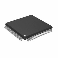
AD8113JSTZ Analog Devices Inc, AD8113JSTZ Datasheet - Page 15

AD8113JSTZ
Manufacturer Part Number
AD8113JSTZ
Description
IC VIDEO CROSSPOINT SWIT 100LQFP
Manufacturer
Analog Devices Inc
Datasheet
1.AD8113JSTZ.pdf
(28 pages)
Specifications of AD8113JSTZ
Function
Video Crosspoint Switch
Circuit
1 x 16:16
Voltage Supply Source
Dual Supply
Voltage - Supply, Single/dual (±)
±4.5 V ~ 12.6 V
Operating Temperature
0°C ~ 70°C
Mounting Type
Surface Mount
Package / Case
100-LQFP
Crosspoint Switch Type
Analog
Control Interface
Parallel, Serial
Supply Voltage Range
4.5V To 5.5V, 4.5V To 12.6V
Operating Temperature Range
0°C To +70°C
Digital Ic Case Style
LQFP
Lead Free Status / RoHS Status
Lead free / RoHS Compliant
Available stocks
Company
Part Number
Manufacturer
Quantity
Price
Company:
Part Number:
AD8113JSTZ
Manufacturer:
ADI
Quantity:
160
Company:
Part Number:
AD8113JSTZ
Manufacturer:
Analog Devices Inc
Quantity:
10 000
Part Number:
AD8113JSTZ
Manufacturer:
ADI/亚德诺
Quantity:
20 000
CALCULATION OF POWER DISSIPATION
The above curve was calculated from
As an example, if the AD8113 is enclosed in an environment at
50°C (T
conditions must not be allowed to exceed 2.5 W.
When calculating on-chip power dissipation, it is necessary to
include the rms current being delivered to the load, multiplied
by the rms voltage drop on the AD8113 output devices. The
dissipation of the on-chip, 4 kΩ feedback resistor network must
also be included. For a sinusoidal output, the on-chip power
dissipation due to the load and feedback network can be approxi-
mated by
For nonsinusoidal output, the power dissipation should be cal-
culated by integrating the on-chip voltage drop multiplied by the
load current over one period.
The user may subtract the quiescent current for the Class AB
output stage when calculating the loaded power dissipation. For
each output stage driving a load, subtract a quiescent power
according to
For the AD8113, I
For each disabled output, the quiescent power supply current in
AV
there is a power dissipation in the on-chip feedback resistors if
the disabled output is being driven from an external source.
REV. A
P
D MAX
,
CC
Figure 6. Maximum Power Dissipation vs. Ambient
Temperature
and AV
2.0
4.0
3.5
2.5
3.0
A
=
), the total on-chip dissipation under all load and supply
P
0
(
AV
D OUTPUT
P
,
EE
D MAX
CC
,
10
drops by approximately 1.25 mA, although
–
O, QUIESCENT
V
OUTPUT RMS
=
=
AMBIENT TEMPERATURE – C
20
(
(
T
AV
JU
,
NCTION MAX
CC
30
–
= 0.67 mA.
)
×
AV
,
I
OUTPUT RMS
θ
40
EE
J
A
)
–
×
T
,
I
50
AMBIENT
O QUIESCENT
,
T
J
+
= 150 C
60
V
)
OUTPUT RMS
4 Ω
k
70
,
2
–15–
An example: AD8113, in an ambient temperature of 70°C,
with all 16 outputs driving 6 V rms into 600 Ω loads. Power
supplies are ± 12 V.
Step 1. Calculate power dissipation of AD8113 using data sheet
P
Step 2. Calculate power dissipation from loads.
P
P
There are 16 outputs, so
Step 3. Subtract quiescent output current for number of loads
There are 16 outputs, so
Step 4. Verify that power dissipation does not exceed maximum
From the figure or the equation, this power dissipation is below
the maximum allowed dissipation for all ambient temperatures
approaching 70°C.
NOTE: It can be shown that for a dual supply of ± a, a Class AB
output stage dissipates maximum power into a grounded load
when the output voltage is a/2. So for a ± 12 V supply, the
above example demonstrates the worst-case power dissipation
into 600 Ω. It can be seen from this example that the minimum
load resistance for ± 12 V operation is 600 Ω (for full rated oper-
ating temperature range). For larger safety margins, when the out-
put signal is unknown, loads of 1 kΩ and greater are recommended.
When operating with ± 5 V supplies, this load resistance may be
lowered to 150 Ω.
P
D, QUIESCENT
D, OUTPUT
D, OUTPUT
D, QUIESCENT
P
D, ON-CHIP
P
DQ, OUTPUT
quiescent currents.
(assumes output voltage >> 0.5 V).
allowed value.
P
P
= (AV
= (12 V – 6 V) × 6 V/600 Ω + (6 V )
D, ON-CHIP
DQ, OUTPUT
= (AV
Figure 7. Simplified Output Stage
= (12 V × 54 mA) + (–12 V × –54 mA)
nP
nP
= P
CC
D, OUTPUT
D, OUTPUT
= (12 V – (–12 V)) × 0.67 mA = 16 mW
CC
D, QUIESCENT
– V
QNPN
QPNP
= 1.3 W + 1.1 W – 0.3 W = 2.1 W
× I
= (AV
OUTPUT, RMS
AVCC
= 16 × 69 mW = 1.1 W
= 16 × 16 mW = 0.3 W
AV
AV
CC
) + (AV
I
4k
I
CC
O, QUIESCENT
EE
O, QUIESCENT
RF
+ nP
– AV
) × I
D, OUTPUT
EE
EE
V
I
OUTPUT
OUTPUT
AGND
OUTPUT, RMS
) × I
× I
AVEE
O, QUIESCENT
– nP
) + (DV
2
+ (5 V × 13 mA)
/4 kΩ = 69 mW
AD8113
+ V
DQ, OUTPUT
OUTPUT
CC
× I
2
DVCC
/4 k Ω
)


