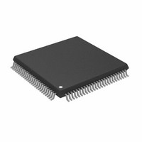
AD8113JSTZ Analog Devices Inc, AD8113JSTZ Datasheet - Page 14

AD8113JSTZ
Manufacturer Part Number
AD8113JSTZ
Description
IC VIDEO CROSSPOINT SWIT 100LQFP
Manufacturer
Analog Devices Inc
Datasheet
1.AD8113JSTZ.pdf
(28 pages)
Specifications of AD8113JSTZ
Function
Video Crosspoint Switch
Circuit
1 x 16:16
Voltage Supply Source
Dual Supply
Voltage - Supply, Single/dual (±)
±4.5 V ~ 12.6 V
Operating Temperature
0°C ~ 70°C
Mounting Type
Surface Mount
Package / Case
100-LQFP
Crosspoint Switch Type
Analog
Control Interface
Parallel, Serial
Supply Voltage Range
4.5V To 5.5V, 4.5V To 12.6V
Operating Temperature Range
0°C To +70°C
Digital Ic Case Style
LQFP
Lead Free Status / RoHS Status
Lead free / RoHS Compliant
Available stocks
Company
Part Number
Manufacturer
Quantity
Price
Company:
Part Number:
AD8113JSTZ
Manufacturer:
ADI
Quantity:
160
Company:
Part Number:
AD8113JSTZ
Manufacturer:
Analog Devices Inc
Quantity:
10 000
Part Number:
AD8113JSTZ
Manufacturer:
ADI/亚德诺
Quantity:
20 000
AD8113
THEORY OF OPERATION
The AD8113 is a gain-of-two crosspoint array with 16 outputs,
each of which can be connected to any one of 16 inputs. Organized
by output row, 16 switchable transconductance stages are
connected to each output buffer in the form of a 16-to-1
multiplexer. Each of the 16 rows of transconductance stages
are wired in parallel to the 16 input pins, for a total array of
256 transconductance stages. Decoding logic for each output
selects one (or none) of the transconductance stages to drive the
output stage. The transconductance stages are NPN input
differential pairs, sourcing current into the folded cascode
output stage. The compensation networks and emitter follower
output buffers are in the output stage. Voltage feedback sets the
gain at +2.
When operated with ± 12 V supplies, this architecture provides
± 10 V drive for 600 Ω audio loads with extremely low distortion
(<0.002%) at audio frequencies. Provided the supplies are lowered
to ± 5 V (to limit power consumption), the AD8113 can drive
reverse-terminated video loads, swinging ± 3.0 V into 150 Ω.
Disabling unused outputs and transconductance stages minimizes
on-chip power consumption.
Features of the AD8113 facilitate the construction of larger
switch matrices. The unused outputs can be disabled, leaving
only a feedback network resistance of 4 kΩ on the output. This
allows multiple ICs to be bused together, provided the output
load impedance is greater than minimum allowed values. Because
no additional input buffering is necessary, high input resistance
and low input capacitance are easily achieved without additional
signal degradation.
The AD8113 inputs have a unique bias current compensation
scheme that overcomes a problem common to transconductance
input array architectures. Typically, input bias current increases
as more and more transconductance stages connected to the same
input are turned on. Anywhere from zero to 16 transconductance
stages can be sharing one input pin, so there is a varying amount
of bias current supplied through the source impedance driving
–14–
the input. For audio systems with larger source impedances,
this has the potential of creating large offset voltages, audible
as pops when switching between channels. The AD8113 samples
and cancels the input bias current contributions from each
transconductance stage so that the residual bias current is nomi-
nally zero regardless of the number of enabled inputs.
Due to the flexibility in allowed supply voltages, internal crosstalk
isolation clamps have variable bias levels. These levels were
chosen to allow for the necessary input range to accommodate
the full output swing with a gain of two. Overdriving the inputs
beyond the device’s linear range will eventually forward bias
these clamps, increasing power dissipation. The valid input
range for ± 12 V supplies is ± 5 V. The valid input range for
± 5 V supplies is ± 1.5 V. When outputs are disabled and being
driven externally, the voltage applied to them should not exceed
the valid output swing range for the AD8113. Exceeding ± 10.5 V
on the outputs of the AD8113 may apply a large differential voltage
on the unused transconductance stages and should be avoided.
A flexible TTL compatible logic interface simplifies the program-
ming of the matrix. Either parallel or serial loading into a first
rank of latches programs each output. A global latch simulta-
neously updates all outputs. In serial mode, a serial-out pin allows
devices to be daisy chained together for single pin programming
of multiple ICs. A power-on reset pin is available to avoid bus
conflicts by disabling all outputs.
Regardless of the supply voltage applied to the AV
pins, the digital logic requires 5 V on the DV
to DGND. In order for the digital-to-analog interface to work
properly, DV
ESD protection diodes require that the DGND and AGND pins
be at the same potential.
CC
must be at least 7 V above AV
CC
EE
. Finally, internal
pin with respect
CC
and AV
REV. A
EE


