ADG509ATQ Analog Devices Inc, ADG509ATQ Datasheet - Page 11
ADG509ATQ
Manufacturer Part Number
ADG509ATQ
Description
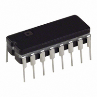
IC MULTIPLEXER DUAL 4X1 16CDIP
Manufacturer
Analog Devices Inc
Type
Analog Multiplexerr
Datasheet
1.ADG509AKRZ-REEL7.pdf
(16 pages)
Specifications of ADG509ATQ
Rohs Status
RoHS non-compliant
Function
Multiplexer
Circuit
2 x 4:1
On-state Resistance
300 Ohm
Voltage Supply Source
Dual Supply
Voltage - Supply, Single/dual (±)
±10.8 V ~ 16.5 V
Current - Supply
20µA
Operating Temperature
-55°C ~ 125°C
Mounting Type
Through Hole
Package / Case
16-CDIP (0.300", 7.62mm)
Msl
MSL 1 - Unlimited
Peak Reflow Compatible (260 C)
No
Leaded Process Compatible
No
Package
16CDIP
Maximum On Resistance
700@16.5V Ohm
Maximum Propagation Delay Bus To Bus
300@±16.5V|450@16.5V ns
Maximum High Level Output Current
20 mA
Multiplexer Architecture
4:1
Number Of Channels Per Chip
1
Maximum Turn-on Time
450@16.5V ns
Power Supply Type
Single|Dual
Lead Free Status / RoHS Status
Contains lead / RoHS non-compliant
Available stocks
Company
Part Number
Manufacturer
Quantity
Price


TEST CIRCUITS
Note: All digital input signal rise and fall times measured from 10% to 90% of 3 V. t
V
S
V1
S
Figure 14. R
R
ON
= V1/I
I
V1
DS
3V
0V
V
V
DD
DD
DS
ON
Figure 17. I
GND
t
TRANSITION
D
V
V
SS
SS
EN
50%
D
90%
D
2.4V
(On)
t
V2
TRANSITION
A
I
ADDRESS
DRIVE (V
D
OUTPUT
(ON)
90%
Figure 19. Switching Time of Multiplexer, t
I
S
(OFF)
IN
)
V1
A
V
V2
IN
Rev. D | Page 11 of 16
Figure 15. I
50Ω
V
V
1
2.4V
DD
DD
SIMILAR CONNECTION FOR ADG509A.
S
(Off)
GND
V
V
SS
SS
A2
A1
A0
EN
EN
ADG508A
V
V
R
TRANSITION
D
0.8V
DD
DD
= t
V1
GND
F
= 20 ns.
V
V
S2–S7
SS
SS
1
S1
S8
D
Figure 18. I
OUTPUT
V
V
ADG509A
V1
DD
DD
1MΩ
V1
V2
GND
DIFF
V
V
SS
SS
ADG508A/ADG509A
EN
= I
V
V
35pF
DB
DD
DD
0.8V
DA
DB
(Off)
Figure 16. I
GND
A
A
V
V
SS
SS
EN
D
V2
D
0.8V
(Off)
V2
A
I
D
(OFF)
Related parts for ADG509ATQ
Image
Part Number
Description
Manufacturer
Datasheet
Request
R

Part Number:
Description:
±1.7g Dual-Axis IMEMS Accelerometer Evaluation Board
Manufacturer:
Analog Devices Inc
Datasheet:

Part Number:
Description:
Inertial Sensor Evaluation System
Manufacturer:
Analog Devices Inc
Datasheet:
Part Number:
Description:
Manufacturer:
Analog Devices Inc
Datasheet:
Part Number:
Description:
Manufacturer:
Analog Devices Inc
Datasheet:
Part Number:
Description:
Manufacturer:
Analog Devices Inc
Datasheet:
Part Number:
Description:
Manufacturer:
Analog Devices Inc
Datasheet:
Part Number:
Description:
Manufacturer:
Analog Devices Inc
Datasheet:
Part Number:
Description:
Manufacturer:
Analog Devices Inc
Datasheet:
Part Number:
Description:
Manufacturer:
Analog Devices Inc
Datasheet:
Part Number:
Description:
Manufacturer:
Analog Devices Inc
Datasheet:
Part Number:
Description:
Manufacturer:
Analog Devices Inc
Datasheet:
Part Number:
Description:
Manufacturer:
Analog Devices Inc
Datasheet:
Part Number:
Description:
Manufacturer:
Analog Devices Inc
Datasheet: