ADG509ATQ Analog Devices Inc, ADG509ATQ Datasheet - Page 7
ADG509ATQ
Manufacturer Part Number
ADG509ATQ
Description
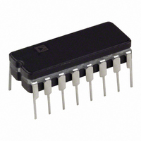
IC MULTIPLEXER DUAL 4X1 16CDIP
Manufacturer
Analog Devices Inc
Type
Analog Multiplexerr
Datasheet
1.ADG509AKRZ-REEL7.pdf
(16 pages)
Specifications of ADG509ATQ
Rohs Status
RoHS non-compliant
Function
Multiplexer
Circuit
2 x 4:1
On-state Resistance
300 Ohm
Voltage Supply Source
Dual Supply
Voltage - Supply, Single/dual (±)
±10.8 V ~ 16.5 V
Current - Supply
20µA
Operating Temperature
-55°C ~ 125°C
Mounting Type
Through Hole
Package / Case
16-CDIP (0.300", 7.62mm)
Msl
MSL 1 - Unlimited
Peak Reflow Compatible (260 C)
No
Leaded Process Compatible
No
Package
16CDIP
Maximum On Resistance
700@16.5V Ohm
Maximum Propagation Delay Bus To Bus
300@±16.5V|450@16.5V ns
Maximum High Level Output Current
20 mA
Multiplexer Architecture
4:1
Number Of Channels Per Chip
1
Maximum Turn-on Time
450@16.5V ns
Power Supply Type
Single|Dual
Lead Free Status / RoHS Status
Contains lead / RoHS non-compliant
Available stocks
Company
Part Number
Manufacturer
Quantity
Price


ABSOLUTE MAXIMUM RATINGS
T
Table 3.
Parameter
V
V
V
Analog Inputs
Continuous Current, S or D
Pulsed Current S or D
Digital Inputs
Power Dissipation (Any Package)
Operating Temperature
Storage Temperature Range
1
Overvoltage at A, EN, S, or D is clamped by diodes. Current should be limited
to the maximum rating shown in Table 3.
DD
DD
SS
A
Voltage at S, D
1 ms Duration, 10% Duty Cycle
Voltage at A, EN
Up to 75°C
Derates Above 75°C by
Commercial (K Version)
Industrial (B Version)
Extended (T Version)
= 25°C, unless otherwise noted.
to GND
to V
to GND
SS
1
1
Ratings
44 V
32 V
–32 V
V
whichever occurs first
20 mA
40 mA
V
whichever occurs first
470 mW
6 mW/°C
−40°C to +85°C
−40°C to +85°C
−55°C to +125°C
−65°C to +150°C
SS
SS
− 2 V to V
− 4 V to V
DD
DD
+ 2 V or 20 mA,
+ 4 V or 20 mA,
Rev. D | Page 7 of 16
Stresses above those listed under Absolute Maximum Ratings
may cause permanent damage to the device. This is a stress
rating only; functional operation of the device at these or any
other conditions above those indicated in the operational
section of this specification is not implied. Exposure to absolute
maximum rating conditions for extended periods may affect
device reliability.
ESD CAUTION
ADG508A/ADG509A
Related parts for ADG509ATQ
Image
Part Number
Description
Manufacturer
Datasheet
Request
R

Part Number:
Description:
±1.7g Dual-Axis IMEMS Accelerometer Evaluation Board
Manufacturer:
Analog Devices Inc
Datasheet:

Part Number:
Description:
Inertial Sensor Evaluation System
Manufacturer:
Analog Devices Inc
Datasheet:
Part Number:
Description:
Manufacturer:
Analog Devices Inc
Datasheet:
Part Number:
Description:
Manufacturer:
Analog Devices Inc
Datasheet:
Part Number:
Description:
Manufacturer:
Analog Devices Inc
Datasheet:
Part Number:
Description:
Manufacturer:
Analog Devices Inc
Datasheet:
Part Number:
Description:
Manufacturer:
Analog Devices Inc
Datasheet:
Part Number:
Description:
Manufacturer:
Analog Devices Inc
Datasheet:
Part Number:
Description:
Manufacturer:
Analog Devices Inc
Datasheet:
Part Number:
Description:
Manufacturer:
Analog Devices Inc
Datasheet:
Part Number:
Description:
Manufacturer:
Analog Devices Inc
Datasheet:
Part Number:
Description:
Manufacturer:
Analog Devices Inc
Datasheet:
Part Number:
Description:
Manufacturer:
Analog Devices Inc
Datasheet: