ADG428BP Analog Devices Inc, ADG428BP Datasheet - Page 5
ADG428BP
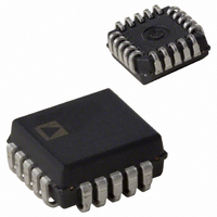
Manufacturer Part Number
ADG428BP
Description
IC MULTIPLEXER 8X1 20PLCC
Manufacturer
Analog Devices Inc
Series
LC²MOSr
Type
Analog Multiplexerr
Datasheet
1.ADG428BRZ.pdf
(12 pages)
Specifications of ADG428BP
Rohs Status
RoHS non-compliant
Function
Multiplexer
Circuit
1 x 8:1
On-state Resistance
100 Ohm
Voltage Supply Source
Single Supply
Voltage - Supply, Single/dual (±)
5V, 12V
Current - Supply
5µA
Operating Temperature
-40°C ~ 85°C
Mounting Type
Surface Mount
Package / Case
20-LCC (J-Lead)
Package
20PLCC
Maximum On Resistance
100@±15V Ohm
Maximum Propagation Delay Bus To Bus
250@±15V|350@12V ns
Maximum High Level Output Current
30 mA
Multiplexer Architecture
8:1
Maximum Turn-on Time
300@12V ns
Power Supply Type
Single|Dual
Available stocks
Company
Part Number
Manufacturer
Quantity
Price

Company:
Part Number:
ADG428BP-REEL
Manufacturer:
Analog Devices Inc
Quantity:
10 000
Company:
Part Number:
ADG428BPZ
Manufacturer:
Analog Devices Inc
Quantity:
10 000
Part Number:
ADG428BPZ
Manufacturer:
ADI/亚德诺
Quantity:
20 000
Company:
Part Number:
ADG428BPZ-REEL
Manufacturer:
Analog Devices Inc
Quantity:
10 000


TERMINOLOGY
V
V
GND
R
I
I
I
V
C
C
C
C
t
t
t
t
V
V
I
Crosstalk
Off Isolation
Charge
Injection
I
I
REV. C
S
D
D
ON
OFF
TRANSITlON
OPEN
INL
DD
SS
R
DD
SS
ON
D
INL
INH
S
D
D
IN
, I
(OFF)
(OFF)
ON
, C
(OFF)
(V
(OFF)
(EN)
S
(I
(EN)
(ON)
S
S
INH
)
(ON)
)
A measure of unwanted signal which is
from the digital input to the analog output
Most positive power supply potential.
Most negative power supply potential in dual
supplies. In single supply applications, it may
be connected to ground.
Ground (0 V) reference.
Ohmic resistance between D and S.
Difference between the R
channels.
Source leakage current when the switch is off.
Drain leakage current when the switch is off.
Channel leakage current when the switch is
on.
Analog voltage on terminals D, S.
Channel input capacitance for “OFF”
condition.
Channel output capacitance for “OFF”
condition.
“ON” switch capacitance.
Digital input capacitance.
Delay time between the 50% and 90% points
of the digital input and switch “ON”
condition.
Delay time between the 50% and 90% points
of the digital input and switch “OFF”
condition.
Delay time between the 50% and 90% points
of the digital inputs and the switch “ON”
condition when switching from one address
state to another.
“OFF” time measured between 80% points of
both switches when switching from one
address state to another.
Maximum input voltage for Logic “0.”
Minimum input voltage for Logic “1.”
Input current of the digital input.
coupled through from one channel to another
as a result of parasitic capacitance.
A measure of unwanted signal coupling
through an “OFF” channel.
A measure of the glitch impulse transferred
during switching.
Positive supply current.
Negative supply current.
ON
of any two
–5–
A2
Latching
X
Reset
X
Transparent Operation
X
0
0
0
0
1
1
1
1
A1
Latching
X
Reset
X
Transparent Operation
X
0
0
1
1
A1
X
X
X
0
0
1
1
0
0
1
1
A0
X
X
X
0
1
0
1
A0
X
X
X
0
1
0
1
0
1
0
1
EN
X
X
0
1
1
1
1
EN
X
X
0
1
1
1
1
1
1
1
1
ADG428 Truth Table
ADG429 Truth Table
WR
g
X
0
0
0
0
0
WR
g
X
0
0
0
0
0
0
0
0
0
RS
1
0
1
1
1
1
1
ADG428/ADG429
RS
1
0
1
1
1
1
1
1
1
1
1
ON SWITCH PAIR
Maintains Previous
Switch Condition
NONE
(Latches Cleared)
NONE
1
2
3
4
ON SWITCH
Maintains Previous
Switch Condition
NONE
(Latches Cleared)
NONE
1
2
3
4
5
6
7
8
Related parts for ADG428BP
Image
Part Number
Description
Manufacturer
Datasheet
Request
R

Part Number:
Description:
±1.7g Dual-Axis IMEMS Accelerometer Evaluation Board
Manufacturer:
Analog Devices Inc
Datasheet:

Part Number:
Description:
Inertial Sensor Evaluation System
Manufacturer:
Analog Devices Inc
Datasheet:
Part Number:
Description:
Manufacturer:
Analog Devices Inc
Datasheet:
Part Number:
Description:
Manufacturer:
Analog Devices Inc
Datasheet:
Part Number:
Description:
Manufacturer:
Analog Devices Inc
Datasheet:
Part Number:
Description:
Manufacturer:
Analog Devices Inc
Datasheet:
Part Number:
Description:
Manufacturer:
Analog Devices Inc
Datasheet:
Part Number:
Description:
Manufacturer:
Analog Devices Inc
Datasheet:
Part Number:
Description:
Manufacturer:
Analog Devices Inc
Datasheet:
Part Number:
Description:
Manufacturer:
Analog Devices Inc
Datasheet:
Part Number:
Description:
Manufacturer:
Analog Devices Inc
Datasheet:
Part Number:
Description:
Manufacturer:
Analog Devices Inc
Datasheet:
Part Number:
Description:
Manufacturer:
Analog Devices Inc
Datasheet: