ADG428BP Analog Devices Inc, ADG428BP Datasheet

IC MULTIPLEXER 8X1 20PLCC

ADG428BP

Manufacturer Part Number
ADG428BP
Description
IC MULTIPLEXER 8X1 20PLCC
Manufacturer
Analog Devices Inc
Series
LC²MOSr
Type
Analog Multiplexerr
Datasheet

Specifications of ADG428BP

Rohs Status
RoHS non-compliant
Function
Multiplexer
Circuit
1 x 8:1
On-state Resistance
100 Ohm
Voltage Supply Source
Single Supply
Voltage - Supply, Single/dual (±)
5V, 12V
Current - Supply
5µA
Operating Temperature
-40°C ~ 85°C
Mounting Type
Surface Mount
Package / Case
20-LCC (J-Lead)
Package
20PLCC
Maximum On Resistance
100@±15V Ohm
Maximum Propagation Delay Bus To Bus
250@±15V|350@12V ns
Maximum High Level Output Current
30 mA
Multiplexer Architecture
8:1
Maximum Turn-on Time
300@12V ns
Power Supply Type
Single|Dual

Available stocks

Company
Part Number
Manufacturer
Quantity
Price
Part Number:
ADG428BP
Manufacturer:
Analog Devices Inc
Quantity:
10 000
Part Number:
ADG428BP
Manufacturer:
AD
Quantity:
1 000
Part Number:
ADG428BP-REEL
Manufacturer:
Analog Devices Inc
Quantity:
10 000
Part Number:
ADG428BPZ
Manufacturer:
Analog Devices Inc
Quantity:
10 000
Part Number:
ADG428BPZ
Manufacturer:
ADI/亚德诺
Quantity:
20 000
Part Number:
ADG428BPZ-REEL
Manufacturer:
Analog Devices Inc
Quantity:
10 000
a
Information furnished by Analog Devices is believed to be accurate and
reliable. However, no responsibility is assumed by Analog Devices for its
use, nor for any infringements of patents or other rights of third parties
which may result from its use. No license is granted by implication or
otherwise under any patent or patent rights of Analog Devices.
GENERAL DESCRIPTION
The ADG428 and ADG429 are monolithic CMOS analog
multiplexers comprising eight single channels and four differen-
tial channels respectively. On-chip address and control latches
facilitate microprocessor interfacing. The ADG428 switches one
of eight inputs to a common output as determined by the 3-bit
binary address lines A0, A1 and A2. The ADG429 switches one
of four differential inputs to a common differential output as
determined by the 2-bit binary address lines A0 and A1. An EN
input on both devices is used to enable or disable the device.
When disabled, all channels are switched OFF. All the control
inputs, address and enable inputs are TTL compatible over the
full specified operating temperature range. This makes the part
suitable for bus-controlled systems such as data acquisition sys-
tems, process controls, avionics and ATEs because the TTL-
compatible address latches simplify the digital interface design
and reduce the board space required.
The ADG428/ADG429 are designed on an enhanced LC
process that provides low power dissipation yet gives high switching
speed and low on resistance. Each channel conducts equally well
in both directions when ON and has an input signal range that
extends to the supplies. In the OFF condition, signal levels up to
the supplies are blocked. All channels exhibit break-before-make
switching action, preventing momentary shorting when switching
channels. Inherent in the design is low charge injection for mini-
mum transients when switching the digital inputs.
The ADG428/ADG429 are improved replacements for the
DG428/DG429 Analog Multiplexers.
REV. C
FEATURES
44 V Supply Maximum Ratings
V
Low On Resistance (60
Low Power Consumption (1.6 mW max)
Low Charge Injection (<4 pC typ)
Fast Switching
Break-Before-Make Switching Action
Plug-In Replacement for DG428/DG429
APPLICATIONS
Automatic Test Equipment
Data Acquisition Systems
Communication Systems
Avionics and Military Systems
Microprocessor Controlled Analog Systems
Medical Instrumentation
SS
to V
DD
Analog Signal Range
typ)
High Performance Analog Multiplexers
2
MOS
LC
PRODUCT HIGHLIGHTS
1. Extended Signal Range
2. Low Power Dissipation
3. Low R
4. Single/Dual Supply Operation
5. Single Supply Operation
One Technology Way, P.O. Box 9106, Norwood, MA 02062-9106, U.S.A.
Tel: 781/329-4700
Fax: 781/326-8703
WR
S8
S1
The ADG428/ADG429 are fabricated on an enhanced
LC
tends to the supply rails.
For applications where the analog signal is unipolar, the
ADG428/ADG429 can be operated from a single rail power
supply. The parts are fully specified with a single +12 V
power supply and will remain functional with single supplies
as low as +5 V.
2
MOS Latchable 4-/8-Channel
2
A2
DECODERS/DRIVERS
MOS process, giving an increased signal range that ex-
ON
ADG428
LATCHES
A1
FUNCTIONAL BLOCK DIAGRAMS
A0
World Wide Web Site: http://www.analog.com
EN
ADG428/ADG429
D
RS
S1A
S4A
S1B
S4B
WR
© Analog Devices, Inc., 1999
DECODERS/DRIVERS
A1
ADG429
LATCHES
A0
EN
DA
DB
RS

Related parts for ADG428BP

ADG428BP Summary of contents

Page 1

FEATURES 44 V Supply Maximum Ratings Analog Signal Range SS DD Low On Resistance (60 typ) Low Power Consumption (1.6 mW max) Low Charge Injection (<4 pC typ) Fast Switching Break-Before-Make Switching Action Plug-In Replacement for ...

Page 2

ADG428/ADG429–SPECIFICATIONS 1 DUAL SUPPLY ( Parameter ANALOG SWITCH Analog Signal Range LEAKAGE CURRENTS Source OFF Leakage I (OFF) S Drain OFF Leakage I (OFF) D ADG428 ADG429 Channel ON Leakage ...

Page 3

SINGLE SUPPLY ( Parameter ANALOG SWITCH Analog Signal Range LEAKAGE CURRENTS Source OFF Leakage I (OFF) S Drain OFF Leakage I (OFF) D ADG428 ADG429 Channel ON Leakage I , ...

Page 4

... Overvoltages at A, EN, WR, RS will be clamped by internal diodes. Current 2 should be limited to the maximum ratings given. ORDERING GUIDE 1 Model Temperature Range ADG428BN – +85 C ADG428BP – +85 C ADG428BR – +85 C ADG428TQ – +125 C ADG429BN – +85 C ADG429BP – +85 C ADG429TQ – ...

Page 5

TERMINOLOGY V Most positive power supply potential Most negative power supply potential in dual SS supplies. In single supply applications, it may be connected to ground. GND Ground (0 V) reference. R Ohmic resistance between D and S. ...

Page 6

ADG428/ADG429 TIMING DIAGRAMS A0, A1, (A2 Figure 1. Figure 1 shows the timing sequence for latching the switch address and enable inputs. The latches are level sensitive; there- fore, ...

Page 7

V = +15V DD 5500 V = –15V SS 5000 4500 4000 3500 3000 2500 2000 1500 1000 500 0 10 100 1k 10k SWITCHING FREQUENCY – Hz Figure 7. Positive Supply Current vs. Switching Frequency 130 V = ...

Page 8

ADG428/ADG429 100 100 1k 10k 100k FREQUENCY – Hz Figure 13. OFF Isolation vs. Frequency 0 +15V –15V +25 C ...

Page 9

TEST CIRCUITS V1 Test Circuit 1. On Resistance (OFF GND Test Circuit ...

Page 10

ADG428/ADG429 3V ENABLE DRIVE 50% – (EN OUTPUT ( 50 OUTPUT 50 OUTPUT 0V 50% t (EN) OFF 0.9V 0.9V ...

Page 11

EN V OUT INJ ADG428 GND Test Circuit 11. OFF Isolation REV OUT ...

Page 12

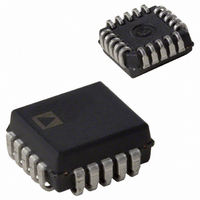
ADG428/ADG429 PLCC (P-20A) 0.180 (4.57) 0.165 (4.19) 0.048 (1.21) 0.056 (1.42) 0.042 (1.07) 0.042 (1.07) 0.048 (1.21 0.042 (1.07 PIN 1 0.050 IDENTIFIER (1.27) TOP VIEW BSC (PINS DOWN 0.020 (0.50) 0.356 ...

Related keywords