ADG333ABNZ Analog Devices Inc, ADG333ABNZ Datasheet - Page 7
ADG333ABNZ
Manufacturer Part Number
ADG333ABNZ
Description
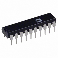
IC SWITCH QUAD SPDT 20DIP
Manufacturer
Analog Devices Inc
Type
Analog Switchr
Datasheet
1.ADG333ABRZ.pdf
(12 pages)
Specifications of ADG333ABNZ
Function
Switch
Circuit
4 x SPDT
On-state Resistance
45 Ohm
Voltage Supply Source
Single Supply
Voltage - Supply, Single/dual (±)
12V
Current - Supply
0.01µA
Operating Temperature
-40°C ~ 85°C
Mounting Type
Through Hole
Package / Case
20-DIP (0.300", 7.62mm)
Analog Switch Type
SPDT
No. Of Channels
4
On State Resistance Max
45ohm
Turn Off Time
80ns
Turn On Time
90ns
Supply Voltage Range
3V To 30V
Operating Temperature Range
-40°C To +85°C
Multiplexer Configuration
Quad SPDT
Number Of Inputs
4
Number Of Outputs
8
Number Of Channels
4
Analog Switch On Resistance
45@±15VOhm
Analog Switch Turn On Time
110ns
Analog Switch Turn Off Time
100ns
Package Type
PDIP N
Power Supply Requirement
Single/Dual
Single Supply Voltage (min)
3V
Single Supply Voltage (typ)
12V
Single Supply Voltage (max)
30V
Dual Supply Voltage (min)
±3V
Dual Supply Voltage (typ)
±5/±9/±12/±15V
Dual Supply Voltage (max)
±20V
Power Dissipation
3.77mW
Supply Current
0.25@±15VmA
Mounting
Through Hole
Pin Count
20
Operating Temp Range
-40C to 85C
Operating Temperature Classification
Industrial
Package
20PDIP N
Maximum On Resistance
45@±15V Ohm
Maximum High Level Output Current
20 mA
Maximum Turn-off Time
100(Typ)@12V ns
Maximum Turn-on Time
110(Typ)@12V ns
Switch Architecture
SPDT
Power Supply Type
Single|Dual
Lead Free Status / RoHS Status
Lead free / RoHS Compliant
Lead Free Status / RoHS Status
Lead free / RoHS Compliant, Lead free / RoHS Compliant
Available stocks
Company
Part Number
Manufacturer
Quantity
Price

Part Number:
ADG333ABNZ
Manufacturer:
ADI/亚德诺
Quantity:
20 000


PIN CONFIGURATIONS AND FUNCTION DESCRIPTIONS
Table 5. Pin Function Descriptions
Pin No.
1, 10, 11, 20
2, 4, 7, 9, 12, 14,
17, 19
3, 8, 13, 18
5
6
15
16
GND
S1A
S1B
S2B
S2A
V
IN1
IN2
Figure 2. PDIP Pin Configuration
D1
D2
SS
10
1
2
3
4
5
6
7
8
9
NC = NO CONNECT
(Not to Scale)
ADG333A
TOP VIEW
Mnemonic
IN1, IN2, IN3, IN4
S1A, S1B, S2B, S2A,
S3A, S3B, S4B, S4A
D1, D2, D3, D4
V
GND
NC
V
SS
DD
20
19
18
17
16
15
14
13
12
11
IN4
S4A
D4
S4B
V
NC
S3B
D3
S3A
IN3
DD
Description
Logic Control Input.
Source Terminal. Can be an input or output.
Drain Terminal. Can be an input or output.
Most Negative Power Supply Potential in Dual Supplies. In single-supply applications, it can be
connected to ground.
Ground (0 V) Reference.
No Connect.
Most Positive Power Supply Potential.
GND
Figure 3. SOIC Pin Configuration
S1A
S1B
S2B
S2A
V
IN1
IN2
D1
D2
SS
10
1
2
3
4
5
6
7
8
9
NC = NO CONNECT
Rev. A | Page 7 of 12
(Not to Scale)
ADG333A
TOP VIEW
20
19
18
17
16
15
14
13
12
11
IN4
S4A
D4
S4B
V
NC
S3B
D3
S3A
IN3
DD
GND
S1A
S1B
S2B
S2A
V
IN1
IN2
D1
D2
SS
Figure 4. SSOP Pin Configuration
10
1
2
3
4
5
6
7
8
9
NC = NO CONNECT
(Not to Scale)
ADG333A
TOP VIEW
20
19
18
17
16
15
14
13
12
11
ADG333A
IN4
S4A
D4
S4B
V
NC
S3B
D3
S3A
IN3
DD
Related parts for ADG333ABNZ
Image
Part Number
Description
Manufacturer
Datasheet
Request
R

Part Number:
Description:
±1.7g Dual-Axis IMEMS Accelerometer Evaluation Board
Manufacturer:
Analog Devices Inc
Datasheet:

Part Number:
Description:
Inertial Sensor Evaluation System
Manufacturer:
Analog Devices Inc
Datasheet:
Part Number:
Description:
Manufacturer:
Analog Devices Inc
Datasheet:
Part Number:
Description:
Manufacturer:
Analog Devices Inc
Datasheet:
Part Number:
Description:
Manufacturer:
Analog Devices Inc
Datasheet:
Part Number:
Description:
Manufacturer:
Analog Devices Inc
Datasheet:
Part Number:
Description:
Manufacturer:
Analog Devices Inc
Datasheet:
Part Number:
Description:
Manufacturer:
Analog Devices Inc
Datasheet:
Part Number:
Description:
Manufacturer:
Analog Devices Inc
Datasheet:
Part Number:
Description:
Manufacturer:
Analog Devices Inc
Datasheet:
Part Number:
Description:
Manufacturer:
Analog Devices Inc
Datasheet:
Part Number:
Description:
Manufacturer:
Analog Devices Inc
Datasheet:
Part Number:
Description:
Manufacturer:
Analog Devices Inc
Datasheet: