ADG333ABNZ Analog Devices Inc, ADG333ABNZ Datasheet - Page 4
ADG333ABNZ
Manufacturer Part Number
ADG333ABNZ
Description
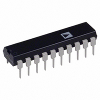
IC SWITCH QUAD SPDT 20DIP
Manufacturer
Analog Devices Inc
Type
Analog Switchr
Datasheet
1.ADG333ABRZ.pdf
(12 pages)
Specifications of ADG333ABNZ
Function
Switch
Circuit
4 x SPDT
On-state Resistance
45 Ohm
Voltage Supply Source
Single Supply
Voltage - Supply, Single/dual (±)
12V
Current - Supply
0.01µA
Operating Temperature
-40°C ~ 85°C
Mounting Type
Through Hole
Package / Case
20-DIP (0.300", 7.62mm)
Analog Switch Type
SPDT
No. Of Channels
4
On State Resistance Max
45ohm
Turn Off Time
80ns
Turn On Time
90ns
Supply Voltage Range
3V To 30V
Operating Temperature Range
-40°C To +85°C
Multiplexer Configuration
Quad SPDT
Number Of Inputs
4
Number Of Outputs
8
Number Of Channels
4
Analog Switch On Resistance
45@±15VOhm
Analog Switch Turn On Time
110ns
Analog Switch Turn Off Time
100ns
Package Type
PDIP N
Power Supply Requirement
Single/Dual
Single Supply Voltage (min)
3V
Single Supply Voltage (typ)
12V
Single Supply Voltage (max)
30V
Dual Supply Voltage (min)
±3V
Dual Supply Voltage (typ)
±5/±9/±12/±15V
Dual Supply Voltage (max)
±20V
Power Dissipation
3.77mW
Supply Current
0.25@±15VmA
Mounting
Through Hole
Pin Count
20
Operating Temp Range
-40C to 85C
Operating Temperature Classification
Industrial
Package
20PDIP N
Maximum On Resistance
45@±15V Ohm
Maximum High Level Output Current
20 mA
Maximum Turn-off Time
100(Typ)@12V ns
Maximum Turn-on Time
110(Typ)@12V ns
Switch Architecture
SPDT
Power Supply Type
Single|Dual
Lead Free Status / RoHS Status
Lead free / RoHS Compliant
Lead Free Status / RoHS Status
Lead free / RoHS Compliant, Lead free / RoHS Compliant
Available stocks
Company
Part Number
Manufacturer
Quantity
Price

Part Number:
ADG333ABNZ
Manufacturer:
ADI/亚德诺
Quantity:
20 000


ADG333A
SINGLE SUPPLY
V
Table 2.
Parameter
ANALOG SWITCH
LEAKAGE CURRENTS
DIGITAL INPUTS
DYNAMIC CHARACTERISTICS
POWER REQUIREMENTS
1
2
Temperature range is as follows: B Version: −40°C to +85°C.
Guaranteed by design; not subject to production test.
DD
Analog Signal Range
RON
Source OFF Leakage I
Channel ON Leakage I
Input High Voltage, V
Input Low Voltage, V
Input Current
I
t
t
Break-Before-Make Delay, t
Charge Injection
OFF Isolation
Channel-to-Channel Crosstalk
C
C
I
V
INL
DD
ON
OFF
S
D
DD
= +12 V, V
, C
(OFF)
or I
S
(ON)
INH
SS
= 0 V ± 10%, GND = 0 V, unless otherwise noted.
INL
S
INH
D
(OFF)
, I
S
(ON)
2
OPEN
+25°C
35
±0.1
±0.25
±0.1
±0.4
110
100
10
5
72
85
12
25
0.05
0.25
−40°C to +85°C
0 V to V
75
±3
±5
2.4
0.8
±0.005
±0.5
200
180
0.35
±3/±30
DD
Rev. A | Page 4 of 12
1
ns max
ns max
mA max
Unit
V
Ω typ
Ω max
nA typ
nA max
nA typ
nA max
V min
V max
µA typ
µA max
ns typ
ns typ
ns min
ns min
pC typ
dB typ
dB typ
pF typ
pF typ
mA typ
V min/V max
Test Conditions/Comments
V
V
V
Figure 15
V
Figure 16
V
R
V
R
V
R
V
V
V
R
V
R
V
V
Digital inputs = 0 V or 5 V
D
DD
D
S
IN
L
S
L
S
L
S
D
DD
L
S
L
S
DD
= V
= 300 Ω, C
= 8 V; Figure 17
= 300 Ω, C
= 8 V; Figure 17
= 300 Ω, C
= 5 V; Figure 18
= 75 Ω, C
= 1.15 V rms; Figure 20
= 75 Ω, C
= 1.15 V rms; Figure 21
= 1 V, 10 V, I
= 12.2 V/1 V, V
= 6 V, R
= 0 V or V
= 13.2 V
= 12 V, V
= 13.5 V
D
= 12.2 V/1 V
D
= 0 W, C
L
L
SS
DD
L
L
L
= 5 pF, f = 1 MHz;
= 5 pF, f = 1 MHz;
= 35 pF;
= 35 pF;
= 35 pF;
= 0 V; Figure 19
S
= –1 mA
S
= 1 V/12.2 V
L
= 10 nF;
Related parts for ADG333ABNZ
Image
Part Number
Description
Manufacturer
Datasheet
Request
R

Part Number:
Description:
±1.7g Dual-Axis IMEMS Accelerometer Evaluation Board
Manufacturer:
Analog Devices Inc
Datasheet:

Part Number:
Description:
Inertial Sensor Evaluation System
Manufacturer:
Analog Devices Inc
Datasheet:
Part Number:
Description:
Manufacturer:
Analog Devices Inc
Datasheet:
Part Number:
Description:
Manufacturer:
Analog Devices Inc
Datasheet:
Part Number:
Description:
Manufacturer:
Analog Devices Inc
Datasheet:
Part Number:
Description:
Manufacturer:
Analog Devices Inc
Datasheet:
Part Number:
Description:
Manufacturer:
Analog Devices Inc
Datasheet:
Part Number:
Description:
Manufacturer:
Analog Devices Inc
Datasheet:
Part Number:
Description:
Manufacturer:
Analog Devices Inc
Datasheet:
Part Number:
Description:
Manufacturer:
Analog Devices Inc
Datasheet:
Part Number:
Description:
Manufacturer:
Analog Devices Inc
Datasheet:
Part Number:
Description:
Manufacturer:
Analog Devices Inc
Datasheet:
Part Number:
Description:
Manufacturer:
Analog Devices Inc
Datasheet: