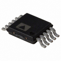
ADG836LYRM Analog Devices Inc, ADG836LYRM Datasheet - Page 5

ADG836LYRM
Manufacturer Part Number
ADG836LYRM
Description
IC SWITCH DUAL SPDT 10MSOP
Manufacturer
Analog Devices Inc
Datasheet
1.ADG836LYRMZ.pdf
(16 pages)
Specifications of ADG836LYRM
Function
Switch
Circuit
2 x SPDT
On-state Resistance
650 mOhm
Voltage Supply Source
Single Supply
Voltage - Supply, Single/dual (±)
1.65 V ~ 3.6 V
Current - Supply
0.003µA
Operating Temperature
-40°C ~ 125°C
Mounting Type
Surface Mount
Package / Case
10-TFSOP, 10-MSOP (0.118", 3.00mm Width)
Lead Free Status / RoHS Status
Contains lead / RoHS non-compliant
Available stocks
Company
Part Number
Manufacturer
Quantity
Price
Part Number:
ADG836LYRM
Manufacturer:
ADI/亚德诺
Quantity:
20 000
Company:
Part Number:
ADG836LYRMZ
Manufacturer:
NSC
Quantity:
327
Table 3. V
Parameter
ANALOG SWITCH
LEAKAGE CURRENTS
DIGITAL INPUTS
DYNAMIC CHARACTERISTICS
Total Harmonic Distortion
POWER REQUIREMENTS
1
2
Temperature range for Y version is −40°C to +125°C.
Guaranteed by design, not subject to production test.
Analog Signal Range
On Resistance (R
On Resistance Match between
Source Off Leakage I
Channel On Leakage I
Input High Voltage, V
Input Low Voltage, V
Input Current
C
t
t
Break-before-Make Time Delay
Charge Injection
Off Isolation
Channel-to-Channel Crosstalk
(THD + N)
Insertion Loss
–3 dB Bandwidth
C
C
I
DD
ON
OFF
(t
IN
S
D
Channels (∆R
I
, C
BBM
(OFF)
, Digital Input Capacitance
INL
S
or I
)
(ON)
DD
INH
= 1.65 V ± 1.95 V, GND = 0 V, unless otherwise noted.
ON
ON
)
)
S
INL
INH
(OFF)
D
, I
S
(ON)
2
+25°C
1
1.4
2
0.1
±0.2
±0.4
±0.2
±0.6
0.005
4
28
37
7
9
21
20
−67
−90
−67
0.14
−0.08
57
25
75
0.003
−40°C – +85°C
2.2
4
±4
±10
38
10
1.0
Rev. A | Page 5 of 16
−40°C – +125°C
0 V to V
2.2
4
±25
±75
0.65 V
0.35 V
±0.1
39
11
5
4
1
DD
DD
DD
Unit
V
Ω typ
Ω max
Ω typ
Ω typ
nA typ
nA max
nA typ
nA max
V min
V max
µA typ
µA max
pF typ
ns typ
ns max
ns typ
ns max
ns typ
ns min
pC typ
dB typ
dB typ
dB typ
%
dB typ
MHz typ
pF typ
pF typ
µA typ
µA max
Test Conditions/Comments
V
V
V
V
V
V
V
R
V
R
V
R
V
V
R
S1A−S2A/S1B−S2B;
R
S1A−S1B/S2A−S2B;
R
R
V
R
R
V
Digital inputs = 0 V or 1.95 V
(Figure 18)
(Figure 19)
(Figure 24)
(Figure 27)
(Figure 25)
DD
DD
DD
DD
S
S
IN
L
S
L
S
L
S1
S
L
L
L
L
S
L
L
DD
= 50 Ω, C
= 50 Ω, C
= 50 Ω, C
= 50 Ω, C
= 50 Ω, C
= 50 Ω, C
= 32 Ω, f = 20 Hz to 20 kHz,
= 50 Ω, C
= 50 Ω, C
= 0.6 V/1.65 V, V
= V
= 1.5 Ω/0 V (Figure 21)
= 1.5 V (Figure 21)
= 1 V, R
= 1.2 V p-p
= V
= V
= 1.8 V, V
= 1.65 V, V
= 1.65 V, V
= 1.95 V
= 1.95 V
D
INL
S2
= 0.6 V or 1.65 V Figure 20
= 1 V (Figure 22)
or V
S
= 0 V, C
L
L
L
L
L
L
L
L
= 5 pF, f = 100 kHz
= 35 pF
= 35 pF
= 35 pF
= 5 pF, f = 100 kHz,
= 5 pF, f = 100 kHz
= 5 pF (Figure 25)
= 5 pF (Figure 25)
S
INH
= 0 V to V
S
S
= 0 V to V
= 0.7 V, I
D
L
= 1 nF (Figure 23)
= 1.65 V/0.6 V
DD
S
DD
= 10 mA
, I
ADG836L
, I
S
= 10 mA
S
= 10 mA


