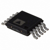
ADG836LYRM Analog Devices Inc, ADG836LYRM Datasheet

ADG836LYRM
Specifications of ADG836LYRM
Available stocks
Related parts for ADG836LYRM
ADG836LYRM Summary of contents
Page 1
FEATURES 0.5 Ω typical on resistance 0.8 Ω maximum on resistance at 125°C 1. 3.6 V operation Automotive temperature range: –40°C to +125°C Guaranteed leakage specifications up to 125°C High current carrying capability: 300 mA continuous Rail-to-rail switching ...
Page 2
ADG836L TABLE OF CONTENTS Specifications..................................................................................... 3 Absolute Maximum Ratings............................................................ 6 Truth Table ........................................................................................ 6 Pin Terminology ............................................................................... 7 Typical Performance Characteristics ............................................. 8 Test Circuits..................................................................................... 11 Outline Dimensions ....................................................................... 13 Ordering Guide........................................................................... 14 REVISION HISTORY 5/04—Data Sheet Changed from Rev. ...
Page 3
SPECIFICATIONS Table 2 3.6 V, GND = 0 V, unless otherwise noted. DD Parameter +25°C ANALOG SWITCH Analog Signal Range On Resistance (R ) 0.5 ON 0.65 On Resistance Match between 0.04 Channels (∆R ) ...
Page 4
ADG836L Table 2.5 V ± 0.2 V, GND = 0 V, unless otherwise noted. DD Parameter +25°C ANALOG SWITCH Analog Signal Range On Resistance (R ) 0.65 ON 0.72 On Resistance Match between 0.04 Channels (∆R ) ...
Page 5
Table 1.65 V ± 1.95 V, GND = 0 V, unless otherwise noted. DD Parameter +25°C ANALOG SWITCH Analog Signal Range On Resistance ( 1 Resistance Match between 0.1 Channels (∆R ) ...
Page 6
ADG836L ABSOLUTE MAXIMUM RATINGS T = 25°C, unless otherwise noted. A Table 4. Parameter Rating V to GND −0 +4 Analog Inputs −0 Digital Inputs −0 4 ...
Page 7
PIN TERMINOLOGY Table 6. Mnemonic Description V Most positive power supply potential Positive supply current. DD GND Ground (0 V) reference. S Source terminal. May be an input or output. D Drain terminal. May be an input or ...
Page 8
ADG836L TYPICAL PERFORMANCE CHARACTERISTICS 0. 25° 0.50 0.45 0. 3.6V DD 0.35 0.30 0.25 0.20 0 0.5 1.0 1 Figure 3. On Resistance ...
Page 9
–20 I –40 –60 – TEMPERATURE (°C) Figure 9. Leakage Current vs. Temperature 2. ...
Page 10
ADG836L 0 – 25° 3.3V/2.5V/1.8V CC –20 –30 –40 –50 –60 –70 –80 0.01 0 FREQUENCY (MHz) Figure 15. Off Isolation vs. Frequency –10 S1A–S1B – 25°C A – ...
Page 11
TEST CIRCUITS V1 Figure 18. On Resistance V 0.1µF V S1B V S S1A IN GND V DD 0.1µ S1B V S S1A IN GND D V ...
Page 12
ADG836L V DD 0.1µ S1B S1A 50Ω GND V OUT OFF ISOLATION = 20 LOG VS Figure 24. Off Isolation V DD 0.1µ S1B S1A D GND V OUT INSERTION LOSS = 20 LOG ...
Page 13
OUTLINE DIMENSIONS 3.00 BSC 10 6 4.90 BSC 3.00 BSC 1 5 PIN 1 0.50 BSC 0.95 0.85 1.10 MAX 0.75 0.15 0.27 SEATING 0.23 0.00 0.17 PLANE 0.08 COPLANARITY 0.10 COMPLIANT TO JEDEC STANDARDS MO-187BA Figure 28. 10-Lead Mini ...
Page 14
... ORDERING GUIDE Model Temperature Range −40°C to +125°C ADG836LYRM −40°C to +125°C ADG836LYRM-REEL −40°C to +125°C ADG836LYRM-REEL7 Package Description Mini Small Outline Package (MSOP) Mini Small Outline Package (MSOP) Mini Small Outline Package (MSOP) Rev Page Package Option Branding ...
Page 15
NOTES Rev Page ADG836L ...
Page 16
ADG836L NOTES © 2004 Analog Devices, Inc. All rights reserved. Trademarks and registered trademarks are the property of their respective owners. D04753–0–5/04(A) Rev Page ...


