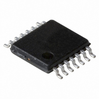
74HC4066PW,112 NXP Semiconductors, 74HC4066PW,112 Datasheet - Page 14

74HC4066PW,112
Manufacturer Part Number
74HC4066PW,112
Description
IC SWITCH QUAD 1X2 14TSSOP
Manufacturer
NXP Semiconductors
Series
74HCr
Datasheet
1.74HC4066N652.pdf
(27 pages)
Specifications of 74HC4066PW,112
Function
Switch
Circuit
4 x 1:2
Voltage Supply Source
Single Supply
Voltage - Supply, Single/dual (±)
2 V ~ 10 V
Current - Supply
40µA
Operating Temperature
-40°C ~ 125°C
Mounting Type
Surface Mount
Package / Case
14-TSSOP (0.173", 4.40mm Width)
Lead Free Status / RoHS Status
Lead free / RoHS Compliant
Other names
568-2697-5
935175000112
935175000112
Philips Semiconductors
Type 74HCT4066
GND = 0 V; t
the output voltage at pins nY or nZ, whichever is assigned as an output.
Note
1. All typical values are measured at T
74HC4066 and 74HCT4066
At recommended conditions and typical values; GND = 0 V; t
whichever is assigned as an input; V
Notes
1. Adjust input voltage V
2. Adjust input voltage V
2004 Nov 11
T
t
t
t
T
t
t
t
d
V
f
C
PHL
PZH
PHZ
PHL
PZH
PHZ
max
sin
SYMBOL
amb
amb
SYMBOL
OFF(feedthr)
ct(s)
ct(p-p)
S
Quad bilateral switches
/t
/t
/t
/t
/t
/t
PLH
PLH
PZL
PLZ
PZL
PLZ
= 40 C to +85 C; note 1
= 40 C to +125 C
r
= t
propagation delay
V
turn-on time nE to V
turn-off time nE to V
propagation delay
V
turn-on time nE to V
turn-off time nE to V
sine wave distortion
switch OFF signal
feed-through
crosstalk between any two
switches
crosstalk voltage between
any input to any switch
(peak-to-peak value)
minimum frequency
response ( 3 dB)
maximum switch
capacitance
f
is
is
= 6 ns; C
to V
to V
PARAMETER
PARAMETER
os
os
is
is
L
is 0 dBM level (0 dBM = 1 mW into 600 ).
is 0 dBM level at V
= 50 pF; V
os
os
os
os
os
is
is the output voltage at pins nY or nZ, whichever is assigned as an output.
amb
is the input voltage at pins nY or nZ, whichever is assigned as an input; V
R
R
R
R
R
R
f = 1 kHz; R
see Fig.17
f = 10 kHz; R
see Fig.17
R
see Figs 11 and 18
R
see Fig.13
R
see Fig.15 (nE, square wave
between V
t
R
and 16
= 25 C.
r
L
L
L
L
L
L
L
L
L
L
= t
os
= ; see Fig.19
= 1 k ; see Figs 20 and 21
= 1 k ; see Figs 20 and 21
= ; see Fig.19
= 1 k ; see Figs 20 and 21
= 1 k ; see Figs 20 and 21
= 600 ; C
= 600 ; C
= 600 ; C
= 50 ; C
f
for 1 MHz (0 dBM = 1 mW into 50 ).
= 6 ns)
CC
L
TEST CONDITIONS
L
L
= 10 k ; C
and GND,
OTHER
OTHER
L
L
L
= 10 pF; see Figs 12
= 10 k ; C
14
= 50 pF; f = 1 MHz;
= 50 pF; f = 1 MHz;
= 50 pF; f = 1 MHz;
r
= t
f
= 6 ns; V
CONDITIONS
L
L
= 50 pF;
= 50 pF;
is
is the input voltage at pins nY or nZ,
74HC4066; 74HCT4066
4.5
4.5
4.5
4.5
4.5
4.5
4.0
8.0
4.0
8.0
note 1
note 1
note 2
V
V
CC
is(p-p)
(V)
(V)
MIN. TYP. MAX. UNIT
4.5
9.0
4.5
9.0
4.5
9.0
4.5
9.0
4.5
9.0
4.5
9.0
V
CC
Product specification
3
12
20
(V)
15
30
44
18
36
53
0.04
0.02
0.12
0.06
110
220
180
200
8
TYP. UNIT
50
50
60
60
ns
ns
ns
ns
ns
ns
%
%
%
%
dB
dB
dB
dB
mV
mV
MHz
MHz
pF
os
is


