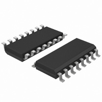
74HC4051D,652 NXP Semiconductors, 74HC4051D,652 Datasheet - Page 4

74HC4051D,652
Manufacturer Part Number
74HC4051D,652
Description
IC MUX/DEMUX 8X1 16SOIC
Manufacturer
NXP Semiconductors
Series
74HCr
Datasheet
1.74HC4051N652.pdf
(31 pages)
Specifications of 74HC4051D,652
Package / Case
16-SOIC (0.154", 3.90mm Width)
Function
Multiplexer/Demultiplexer
Circuit
1 x 8:1
On-state Resistance
60 Ohm
Voltage Supply Source
Single Supply
Voltage - Supply, Single/dual (±)
2 V ~ 10 V
Current - Supply
16µA
Operating Temperature
-40°C ~ 125°C
Mounting Type
Surface Mount
Number Of Channels
1 Channel
On Resistance (max)
180 Ohm @ 4.5 V
On Time (max)
345 ns @ 2 V
Off Time (max)
290 ns @ 2 V
Supply Voltage (max)
10 V
Supply Voltage (min)
2 V
Maximum Power Dissipation
500 mW
Maximum Operating Temperature
+ 125 C
Minimum Operating Temperature
- 40 C
Mounting Style
SMD/SMT
Number Of Switches
Single
Lead Free Status / RoHS Status
Lead free / RoHS Compliant
Lead Free Status / RoHS Status
Lead free / RoHS Compliant, Lead free / RoHS Compliant
Other names
568-3961-5
74HC4051D
74HC4051D
933714820652
74HC4051D
74HC4051D
933714820652
NXP Semiconductors
6. Pinning information
Table 2.
74HC_HCT4051
Product data sheet
Symbol
E
V
GND
S0, S1, S2
Y0, Y1, Y2, Y3, Y4, Y5, Y6, Y7 13, 14, 15, 12, 1, 5, 2, 4 independent input or output
Z
V
Fig 5.
EE
CC
Pin configuration DIP16, SO16, and (T)SSOP16
Pin description
GND
V
Y4
Y6
Y7
Y5
EE
E
Z
1
2
3
4
5
6
7
8
6.1 Pinning
6.2 Pin description
74HCT4051
74HC4051
Pin
6
7
8
11, 10, 9
3
16
001aad539
All information provided in this document is subject to legal disclaimers.
16
15
14
13
12
11
10
9
V
Y2
Y1
Y0
Y3
S0
S1
S2
CC
Rev. 4 — 17 January 2011
Description
enable input (active LOW)
supply voltage
ground supply voltage
select input
common output or input
supply voltage
Fig 6.
(1) This is not a supply pin. The substrate is attached to this
74HC4051; 74HCT4051
8-channel analog multiplexer/demultiplexer
pad using conductive die attach material. There is no
electrical or mechanical requirement to solder this pad.
However, if it is soldered, the solder land should remain
floating or be connected to V
Pin configuration DHVQFN16
index area
terminal 1
V
Y6
Y7
Y5
EE
Z
E
Transparent top view
2
3
4
5
6
7
74HCT4051
74HC4051
V
CC
(1)
CC
.
15
14
13
12
11
10
001aad540
© NXP B.V. 2011. All rights reserved.
Y2
Y1
Y0
Y3
S0
S1
4 of 31


