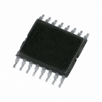
74HCT4316PW,118 NXP Semiconductors, 74HCT4316PW,118 Datasheet - Page 9

74HCT4316PW,118
Manufacturer Part Number
74HCT4316PW,118
Description
IC SWITCH QUAD 1X1 16TSSOP
Manufacturer
NXP Semiconductors
Series
74HCTr
Datasheet
1.74HC4316D653.pdf
(15 pages)
Specifications of 74HCT4316PW,118
Package / Case
16-TSSOP (0.173", 4.40mm Width)
Function
Switch
Circuit
4 x 1:1
On-state Resistance
80 Ohm
Voltage Supply Source
Dual Supply
Voltage - Supply, Single/dual (±)
±4.5 V ~ 5.5 V
Current - Supply
16µA
Mounting Type
Surface Mount
Switch Configuration
SPST
On Resistance (max)
320 Ohm @ 4.5 V
On Time (max)
56 ns @ 4.5 V
Off Time (max)
50 ns @ 4.5 V
Supply Voltage (max)
5.5 V
Supply Voltage (min)
4.5 V
Maximum Power Dissipation
500 mW
Maximum Operating Temperature
+ 125 C
Mounting Style
SMD/SMT
Minimum Operating Temperature
- 40 C
Lead Free Status / RoHS Status
Lead free / RoHS Compliant
Lead Free Status / RoHS Status
Lead free / RoHS Compliant, Lead free / RoHS Compliant
Other names
74HCT4316PW-T
74HCT4316PW-T
935188500118
74HCT4316PW-T
935188500118
Philips Semiconductors
DC CHARACTERISTICS FOR 74HCT
Voltages are referenced to GND (ground = 0)
Note
1. The value of additional quiescent supply current ( I
September 1993
V
V
I
INPUT
nS
E
SYMBOL
CC
I
I
I
I
IH
IL
Quad bilateral switches
I
S
S
CC
To determine I
HIGH level
input voltage
LOW level
input voltage
input leakage
current
analog switch
OFF-state
analog switch
ON-state
quiescent
supply current
additional
quiescent
supply current
per input pin for
unit load
coefficient is 1
(note 1)
PARAMETER
current
current
CC
UNIT LOAD COEFFICIENT
0.50
0.50
per input, multiply this value by the unit load coefficient shown in the table below.
2.0
min.
1.6
1.2
100
typ.
25
max. min. max. min. max.
0.8
0.1
0.1
0.1
8.0
16.0
360
T
74HCT
amb
2.0
40 to 85
( C)
CC
0.8
1.0
1.0
1.0
80.0
160.0
450
) for a unit load of 1 is given here.
9
2.0
40 to 125
0.8
1.0
1.0
1.0
160.0
320.0
490
V
V
UNIT
A
A
A
A
A
4.5
to
5.5
4.5
to
5.5
5.5
10.0
10.0
5.5
5.0
4.5
to
5.5
V
(V)
CC
TEST CONDITIONS
0
0
0
0
0
V
74HC/HCT4316
(V)
5.0
EE
Product specification
V
or
GND
V
or
V
V
or
V
V
or
GND
V
2.1 V
CC
CC
CC
IH
IL
IH
IL
V
I
V
(see Fig.10)
V
(see Fig.11)
V
or V
V
or V
other inputs
at V
GND
V
V
CC
CC
is
OS
OTHER
S
S
= V
CC
CC
EE
= V
=
=
V
V
;
EE
or
EE
EE
CC


