74HC4067DB,118 NXP Semiconductors, 74HC4067DB,118 Datasheet - Page 8
74HC4067DB,118
Manufacturer Part Number
74HC4067DB,118
Description
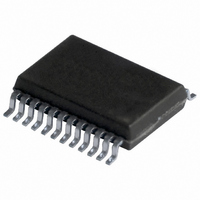
IC MUX/DEMUX 1X16 24SSOP
Manufacturer
NXP Semiconductors
Series
74HCr
Type
Analog Multiplexerr
Datasheet
1.74HCT4067PW112.pdf
(29 pages)
Specifications of 74HC4067DB,118
Package / Case
24-SSOP (0.200", 5.30mm Width)
Function
Multiplexer/Demultiplexer
Circuit
1 x 1:16
On-state Resistance
60 Ohm
Voltage Supply Source
Single Supply
Voltage - Supply, Single/dual (±)
2 V ~ 10 V
Current - Supply
16µA
Operating Temperature
-40°C ~ 125°C
Mounting Type
Surface Mount
Number Of Channels
1 Channel
On Resistance (max)
180 Ohm @ 4.5 V
On Time (max)
300 ns @ 2 V
Off Time (max)
290 ns @ 2 V
Supply Voltage (max)
10 V
Supply Voltage (min)
2 V
Maximum Power Dissipation
500 mW
Maximum Operating Temperature
+ 125 C
Minimum Operating Temperature
- 40 C
Mounting Style
SMD/SMT
Number Of Switches
Single
Package
24SSOP
Maximum On Resistance
180@4.5V Ohm
Maximum Propagation Delay Bus To Bus
75@2V|15@4.5V|13@6V|9@9V ns
Maximum Low Level Output Current
25 mA
Multiplexer Architecture
16:1
Maximum Turn-off Time
290@2V ns
Maximum Turn-on Time
300@2V ns
Power Supply Type
Single
Lead Free Status / RoHS Status
Lead free / RoHS Compliant
Lead Free Status / RoHS Status
Lead free / RoHS Compliant, Lead free / RoHS Compliant
Other names
74HC4067DB-T
74HC4067DB-T
935165200118
74HC4067DB-T
935165200118


NXP Semiconductors
8. Limiting values
Table 4.
In accordance with the Absolute Maximum Rating System (IEC 60134). Voltages are referenced to GND (ground = 0 V).
[1]
[2]
[3]
[4]
[5]
9. Recommended operating conditions
Table 5.
74HC_HCT4067_3
Product data sheet
Symbol
V
I
I
I
I
I
T
P
P
Symbol
74HC4067
V
V
V
t
t
T
IK
SK
SW
CC
GND
r
f
stg
amb
CC
tot
CC
I
SW
To avoid drawing V
switch must not exceed 0.4 V. If the switch current flows into terminal Z, no V
no limit for the voltage drop across the switch, but the voltages at Yn and Z may not exceed V
For DIP24 package: P
For SO24 package: P
For SSOP24 and TSSOP24 packages: P
For DHVQFN24 package: P
Parameter
supply voltage
input clamping current
switch clamping current
switch current
supply current
ground current
storage temperature
total power dissipation
power dissipation
Parameter
supply voltage
input voltage
switch voltage
rise time
fall time
ambient temperature
Limiting values
Recommended operating conditions
CC
tot
current out of terminal Z, when switch current flows in terminals Yn, the voltage drop across the bidirectional
tot
derates linearly with 8 mW/K above 70 C.
derates linearly with 12 mW/K above 70 C.
tot
derates linearly with 4.5 mW/K above 60 C.
tot
derates linearly with 5.5 mW/K above 60 C.
Conditions
V
V
V
T
per switch
Conditions
V
V
V
V
V
V
V
V
amb
I
SW
SW
DIP24 package
SO24 package
SSOP24 package
TSSOP24 package
DHVQFN24 package
< 0.5 V or V
CC
CC
CC
CC
CC
CC
CC
CC
Rev. 03 — 15 October 2007
< 0.5 V or V
= 0.5 V to (V
= 40 C to +125 C
= 2.0 V
= 4.5 V
= 6.0 V
= 10.0 V
= 2.0 V
= 4.5 V
= 6.0 V
= 10.0 V
I
> V
SW
CC
CC
> V
+ 0.5 V)
+ 0.5 V
74HC4067; 74HCT4067
CC
16-channel analog multiplexer/demultiplexer
CC
+ 0.5 V
current will flow out of terminals Yn. In this case there is
Min
2.0
GND
GND
-
-
-
-
-
-
-
-
40
CC
or GND.
[1]
[2]
[3]
[4]
[4]
[5]
Min
-
-
-
-
-
-
-
-
-
-
-
0.5
65
Typ
5.0
-
-
-
6.0
-
-
-
6.0
-
-
+25
© NXP B.V. 2007. All rights reserved.
Max
+11.0
50
+150
750
500
500
500
500
100
20
20
25
50
Max
10.0
V
V
1000
500
400
250
1000
500
400
250
+125
CC
CC
Unit
V
mA
mA
mA
mA
mA
mW
mW
mW
mW
mW
mW
C
Unit
V
V
V
ns
ns
ns
ns
ns
ns
ns
ns
C
8 of 29
Related parts for 74HC4067DB,118
Image
Part Number
Description
Manufacturer
Datasheet
Request
R

Part Number:
Description:
IC MUX/DEMUX 1X16 24SOIC
Manufacturer:
NXP Semiconductors
Datasheet:
Part Number:
Description:
IC MUX/DEMUX 1X16 24SOIC
Manufacturer:
NXP Semiconductors
Datasheet:

Part Number:
Description:
Analog Multiplexer Single 16:1 24-Pin SO Bulk
Manufacturer:
NXP Semiconductors
Datasheet:
Part Number:
Description:
NXP Semiconductors designed the LPC2420/2460 microcontroller around a 16-bit/32-bitARM7TDMI-S CPU core with real-time debug interfaces that include both JTAG andembedded trace
Manufacturer:
NXP Semiconductors
Datasheet:

Part Number:
Description:
NXP Semiconductors designed the LPC2458 microcontroller around a 16-bit/32-bitARM7TDMI-S CPU core with real-time debug interfaces that include both JTAG andembedded trace
Manufacturer:
NXP Semiconductors
Datasheet:
Part Number:
Description:
NXP Semiconductors designed the LPC2468 microcontroller around a 16-bit/32-bitARM7TDMI-S CPU core with real-time debug interfaces that include both JTAG andembedded trace
Manufacturer:
NXP Semiconductors
Datasheet:
Part Number:
Description:
NXP Semiconductors designed the LPC2470 microcontroller, powered by theARM7TDMI-S core, to be a highly integrated microcontroller for a wide range ofapplications that require advanced communications and high quality graphic displays
Manufacturer:
NXP Semiconductors
Datasheet:
Part Number:
Description:
NXP Semiconductors designed the LPC2478 microcontroller, powered by theARM7TDMI-S core, to be a highly integrated microcontroller for a wide range ofapplications that require advanced communications and high quality graphic displays
Manufacturer:
NXP Semiconductors
Datasheet:
Part Number:
Description:
The Philips Semiconductors XA (eXtended Architecture) family of 16-bit single-chip microcontrollers is powerful enough to easily handle the requirements of high performance embedded applications, yet inexpensive enough to compete in the market for hi
Manufacturer:
NXP Semiconductors
Datasheet:
Part Number:
Description:
The XA-S3 device is a member of Philips Semiconductors? XA(eXtended Architecture) family of high performance 16-bitsingle-chip microcontrollers
Manufacturer:
NXP Semiconductors
Datasheet:

Part Number:
Description:
The NXP BlueStreak LH75401/LH75411 family consists of two low-cost 16/32-bit System-on-Chip (SoC) devices
Manufacturer:
NXP Semiconductors
Datasheet:
Part Number:
Description:
The NXP LPC3130/3131 combine an 180 MHz ARM926EJ-S CPU core, high-speed USB2
Manufacturer:
NXP Semiconductors
Datasheet:
Part Number:
Description:
The NXP LPC3141 combine a 270 MHz ARM926EJ-S CPU core, High-speed USB 2
Manufacturer:
NXP Semiconductors
Part Number:
Description:
The NXP LPC3143 combine a 270 MHz ARM926EJ-S CPU core, High-speed USB 2
Manufacturer:
NXP Semiconductors