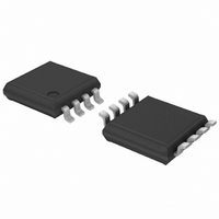
74LVCV2G66DP,125 NXP Semiconductors, 74LVCV2G66DP,125 Datasheet - Page 6

74LVCV2G66DP,125
Manufacturer Part Number
74LVCV2G66DP,125
Description
IC SWITCH DUAL SPST 8TSSOP
Manufacturer
NXP Semiconductors
Datasheet
1.74LVCV2G66DC125.pdf
(23 pages)
Specifications of 74LVCV2G66DP,125
Function
Switch
Circuit
2 x SPST - NO
On-state Resistance
7.3 Ohm
Voltage Supply Source
Single Supply
Voltage - Supply, Single/dual (±)
2.3 V ~ 5.5 V
Current - Supply
0.1µA
Operating Temperature
-40°C ~ 125°C
Mounting Type
Surface Mount
Package / Case
8-TSSOP
Lead Free Status / RoHS Status
Lead free / RoHS Compliant
Other names
74LVCV2G66DP-G
74LVCV2G66DP-G
935274431125
74LVCV2G66DP-G
935274431125
NXP Semiconductors
Table 8.
At recommended operating conditions; voltages are referenced to GND (ground 0 V); for graphs see
[1]
[2]
74LVCV2G66
Product data sheet
Symbol
R
R
R
Fig 6. Test circuit for measuring OFF-state leakage
ON(peak)
ON(rail)
ON(flat)
All typical values are measured at T
Flatness is defined as the difference between the maximum and minimum value of ON resistance measured at identical V
temperature.
current
V
V
I
Resistance R
IL
= GND and V
Parameter
ON resistance
(peak)
ON resistance (rail) V
ON resistance
(flatness)
V I
10.1 Test circuits
10.2 ON resistance
nE
nZ
O
ON
= GND or 5.5 V.
V
CC
GND
Conditions
V
see
V
V
amb
SW
SW
SW
SW
nY
I
I
I
I
I
I
I
I
I
I
I
I
I
I
I
I
SW
SW
SW
SW
SW
SW
SW
SW
SW
SW
SW
SW
SW
SW
SW
SW
Figure 8
= 25 °C and nominal V
= GND to V
= GND; V
= V
= GND to V
= 8 mA; V
= 12 mA; V
= 24 mA; V
= 32 mA; V
= 8 mA; V
= 12 mA; V
= 24 mA; V
= 32 mA; V
= 8 mA; V
= 12 mA; V
= 24 mA; V
= 32 mA; V
= 8 mA; V
= 12 mA; V
= 24 mA; V
= 32 mA; V
I
S
All information provided in this document is subject to legal disclaimers.
001aag488
CC
; V
V O
I
I
= V
= V
Rev. 3 — 16 June 2010
CC
CC
CC
CC
CC
CC
CC
CC
CC
CC
CC
CC
CC
CC
CC
CC
CC
CC
IH
; V
; V
IH
= 2.3 V to 2.7 V
= 2.3 V to 2.7 V
= 2.3 V to 2.7 V
= 2.5 V
= 2.7 V
= 3.0 V to 3.6 V
= 4.5 V to 5.5 V
= 2.7 V
= 3.0 V to 3.6 V
= 4.5 V to 5.5 V
= 2.7 V
= 3.0 V to 3.6 V
= 4.5 V to 5.5 V
= 2.7 V
= 3.3 V
= 5.0 V
; see
I
I
= V
= V
CC
IH
IH
Figure 8
.
;
Fig 7. Test circuit for measuring ON-state leakage
current
V
[2]
I
= 5.5 V or GND and V
V
IH
Min
−40 °C to +85 °C
-
-
-
-
-
-
-
-
-
-
-
-
-
-
-
-
Overvoltage tolerant bilateral switch
V I
I
S
Typ
8.3
7.4
8.5
8.0
7.5
7.3
8.5
7.2
6.5
5.7
13
10
17
10
5
3
nE
nZ
[1]
Max
74LVCV2G66
30
25
20
15
20
18
15
10
20
18
15
10
V
-
-
-
-
O
CC
GND
= open circuit.
−40 °C to +125 °C Unit
Figure 9
Min
nY
-
-
-
-
-
-
-
-
-
-
-
-
-
-
-
-
001aag489
© NXP B.V. 2010. All rights reserved.
V O
and
Max
30
25
20
15
20
18
15
10
20
18
15
10
CC
-
-
-
-
Figure
and
6 of 23
Ω
Ω
Ω
Ω
Ω
Ω
Ω
Ω
Ω
Ω
Ω
Ω
Ω
Ω
Ω
Ω
10.


