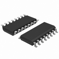
74HCT4316D,118 NXP Semiconductors, 74HCT4316D,118 Datasheet - Page 2

74HCT4316D,118
Manufacturer Part Number
74HCT4316D,118
Description
IC SWITCH QUAD 1X1 16SOIC
Manufacturer
NXP Semiconductors
Series
74HCTr
Datasheet
1.74HC4316D653.pdf
(15 pages)
Specifications of 74HCT4316D,118
Package / Case
16-SOIC (0.154", 3.90mm Width)
Function
Switch
Circuit
4 x 1:1
On-state Resistance
80 Ohm
Voltage Supply Source
Dual Supply
Voltage - Supply, Single/dual (±)
±4.5 V ~ 5.5 V
Current - Supply
16µA
Mounting Type
Surface Mount
Switch Configuration
SPST
On Resistance (max)
320 Ohm @ 4.5 V
On Time (max)
56 ns @ 4.5 V
Off Time (max)
50 ns @ 4.5 V
Supply Voltage (max)
5.5 V
Supply Voltage (min)
4.5 V
Maximum Power Dissipation
500 mW
Maximum Operating Temperature
+ 125 C
Mounting Style
SMD/SMT
Minimum Operating Temperature
- 40 C
Lead Free Status / RoHS Status
Lead free / RoHS Compliant
Lead Free Status / RoHS Status
Lead free / RoHS Compliant, Lead free / RoHS Compliant
Other names
74HCT4316D-T
74HCT4316D-T
933757470118
74HCT4316D-T
933757470118
Philips Semiconductors
FEATURES
GENERAL DESCRIPTION
The 74HC/HCT4316 are high-speed Si-gate CMOS
devices. They are specified in compliance with JEDEC
standard no. 7A.
QUICK REFERENCE DATA
V
Notes
1. C
September 1993
t
t
t
C
C
C
SYMBOL
EE
PZH
PZL
PHZ
Low “ON” resistance:
160
120
Logic level translation:
to enable 5 V logic to communicate
with
Typical “break before make” built in
Output capability: non-standard
I
Quad bilateral switches
I
PD
S
CC
80
dissipation (P
f
f
= GND = 0 V; T
i
o
/ t
PD
= input frequency in MHz
category: MSI
= output frequency in MHz
{ (C
PLZ
P
where:
is used to determine the dynamic power
5 V analog signals
(typ.) at V
(typ.) at V
(typ.) at V
D
L
= C
turn “ON” time
turn “ON” time
turn “OFF” time
input capacitance
power dissipation capacitance per switch
max. switch capacitance
C
PD
S
E to V
nS to V
E to V
nS to V
E to V
nS to V
)
D
CC
CC
CC
V
V
in W):
amb
CC
CC
OS
OS
OS
OS
OS
OS
2
2
V
V
V
= 25 C; t
EE
EE
EE
f
f
i
PARAMETER
o
= 4.5 V
= 6.0 V
= 9.0 V
} = sum of outputs
{ (C
r
= t
L
f
= 6 ns
C
S
) V
CC
2
f
o
}
C
V
CONDITIONS
notes 1 and 2
2
CC
L
= 15 pF; R
The 74HC/HCT4316 have four independent analog
switches. Each switch has two input/output terminals
(nY, nZ) and an active HIGH select input (nS). When the
enable input (E) is HIGH, all four analog switches are
turned off.
Current through a switch will not cause additional V
current provided the voltage at the terminals of the switch
is maintained within the supply voltage range;
V
equivalent terminals.
V
control inputs (E and nS). The V
to 10.0 V for HC and 4.5 to 5.5 V for HCT.
The analog inputs/outputs (nY and nZ) can swing between
V
V
See the “4016” for the version without logic level
translation.
2. For HC the condition is V
= 5 V
CC
CC
CC
CC
C
C
V
For HCT the condition is V
and GND are the supply voltage pins for the digital
as a positive limit and V
CC
L
S
V
= output load capacitance in pF
= max. switch capacitance in pF
EE
(V
= supply voltage in V
L
Y
may not exceed 10.0 V.
, V
= 1 k ;
Z
)
V
19
16
19
16
20
16
3.5
13
5
EE
. Inputs nY and nZ are electrically
HC
TYPICAL
EE
I
I
74HC/HCT4316
as a negative limit.
= GND to V
= GND to V
CC
19
17
24
21
21
19
3.5
14
5
Product specification
to GND ranges are 2.0
HCT
CC
CC
ns
ns
ns
ns
ns
ns
pF
pF
pF
1.5 V
UNIT
CC


