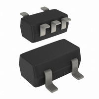
74HCT1G66GW,125 NXP Semiconductors, 74HCT1G66GW,125 Datasheet - Page 9

74HCT1G66GW,125
Manufacturer Part Number
74HCT1G66GW,125
Description
IC SWITCH SPST UMT5
Manufacturer
NXP Semiconductors
Series
74HCTr
Type
Analog Switchr
Datasheet
1.74HC1G66GW125.pdf
(18 pages)
Specifications of 74HCT1G66GW,125
Package / Case
6-TSSOP (5 lead), SC-88A, SOT-353
Function
Switch
Circuit
1 x SPST- NO
Voltage Supply Source
Single Supply
Voltage - Supply, Single/dual (±)
4.5 V ~ 5.5 V
Operating Temperature
-40°C ~ 125°C
Mounting Type
Surface Mount
Switch Configuration
SPST
On Resistance (max)
42 Ohm (Typ) @ 4.5 V
On Time (max)
15 ns (Typ) @ 4.5 V
Off Time (max)
13 ns (Typ) @ 4.5 V
Supply Voltage (max)
5.5 V
Supply Voltage (min)
4.5 V
Maximum Power Dissipation
250 mW
Maximum Operating Temperature
+ 125 C
Mounting Style
SMD/SMT
Minimum Operating Temperature
- 40 C
Package
5TSSOP
Maximum On Resistance
142@4.5V Ohm
Maximum Propagation Delay Bus To Bus
3(Typ)@4.5V ns
Maximum Low Level Output Current
25 mA
Maximum Turn-off Time
13(Typ)@4.5V ns
Maximum Turn-on Time
15(Typ)@4.5V ns
Switch Architecture
SPST
Power Supply Type
Single
Lead Free Status / RoHS Status
Lead free / RoHS Compliant
Lead Free Status / RoHS Status
Lead free / RoHS Compliant, Lead free / RoHS Compliant
Other names
74HCT1G66GW-G
74HCT1G66GW-G
935245760125
74HCT1G66GW-G
935245760125
Available stocks
Company
Part Number
Manufacturer
Quantity
Price
Company:
Part Number:
74HCT1G66GW,125
Manufacturer:
EPCOS
Quantity:
24
NXP Semiconductors
Table 10.
74HC_HCT1G66_4
Product data sheet
Type
74HC1G66
74HCT1G66
Fig 8.
Fig 9.
Measurement points are given in
Logic levels: V
Input (Y or Z) to output (Z or Y) propagation delays
Measurement points are given in
Logic levels: V
Enable and disable times
Measurement points
11.1 Waveforms and test circuit
Input
V
0.5V
1.3 V
OL
OL
M
Y or Z
Y or Z
and V
and V
CC
OH
OH
HIGH-to-OFF
OFF-to-HIGH
OFF-to-LOW
LOW-to-OFF
are typical output voltage levels that occur with the output load.
are typical output voltage levels that occur with the output load.
output
output
Z or Y output
Y or Z input
E
Table
Table
Output
V
0.5V
1.3 V
M
GND
GND
V
V
V
10.
10.
OH
CC
OL
V
CC
GND
V
I
V
Rev. 04 — 19 December 2008
OH
OL
V
I
V
enabled
switch
M
t
t
PLZ
PHZ
V
M
V
V
V
V
M
X
OL
OL
t
V
PLH
X
V
+ 10%
+ 10%
Y
74HC1G66; 74HCT1G66
disabled
switch
Single-pole single-throw analog switch
mna667
t
PZL
t
t
PZH
PHL
V
M
V
M
enabled
V
V
V
switch
mna668
Y
OH
OH
10%
10%
© NXP B.V. 2008. All rights reserved.
9 of 18


