MAX4674ETE+ Maxim Integrated Products, MAX4674ETE+ Datasheet - Page 7

MAX4674ETE+
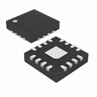
Manufacturer Part Number
MAX4674ETE+
Description
IC MULTIPLEXER QUAD 2X1 16TQFN
Manufacturer
Maxim Integrated Products
Datasheet
1.MAX4674ESE.pdf
(13 pages)
Specifications of MAX4674ETE+
Function
Multiplexer
Circuit
4 x 2:1
On-state Resistance
4 Ohm
Voltage Supply Source
Single Supply
Voltage - Supply, Single/dual (±)
1.8 V ~ 5.5 V
Current - Supply
1µA
Operating Temperature
-40°C ~ 85°C
Mounting Type
Surface Mount
Package / Case
16-TQFN Exposed Pad
Lead Free Status / RoHS Status
Lead free / RoHS Compliant
their leakages will vary as the signal varies. The differ-
ence in the two-diode leakages to the V+ and GND
pins constitutes the analog-signal-path leakage current.
All analog leakage current flows between each pin and
one of the supply terminals, not to the other switch ter-
minal, which is why both sides of a given switch can
show leakage currents of either the same or opposite
polarity.
V+ and GND power the internal logic and set the input
logic limits. Logic inputs have ESD-protection diodes to
ground.
The logic-level thresholds are TTL/CMOS compatible
when V+ is +5V. As V+ rises, the threshold increases;
as V+ falls, the threshold decreases. For example,
when V+ = +3V, the guaranteed minimum logic-high
threshold decreases to 2.0V.
The MAX4674 operates from a single supply between
+1.8V and +5.5V. At room temperature, it actually
“works” with a single supply near or below +1.7V; as
supply voltage decreases, however, switch on-resis-
tance becomes very high.
Proper power-supply sequencing is recommended for
all CMOS devices. Do not exceed the absolute maxi-
mum ratings because stresses beyond the listed rat-
Figure 1. Overvoltage Protection Using External Blocking
Diodes
_______________________________________________________________________________________
*
*
GND
V+
GND
Overvoltage Protection
V+
D1
EXTERNAL
BLOCKING DIODE
D2
EXTERNAL
BLOCKING DIODE
*INTERNAL PROTECTION DIODES
Low-Voltage Operation
*
*
MAX4674
3V/5V, 4Ω, Wideband Quad
ings can cause permanent damage to the device.
Always sequence V+ on first, followed by the logic
inputs and analog signals. If power-supply sequencing
is not possible, add two small signal diodes (D1, D2) in
series with the supply pins for overvoltage protection
(Figure 1).
Adding diodes reduces the analog-signal range to one
diode drop below V+ and one diode drop above GND,
but does not affect the device’s low switch resistance
and low leakage characteristics. Device operation is
unchanged, and the difference between V+ and GND
should not exceed 6V. These protection diodes are not
recommended if signal levels must extend to ground.
In 50Ω systems, signal response is reasonably flat up
to 50MHz (see the Typical Operating Characteristics).
Above 20MHz, the on response has several minor
peaks that are highly layout dependent. The problem is
not turning the switch on, but turning it off. The off-state
switch acts like a capacitor and passes higher frequen-
cies with less attenuation. At 10MHz, off-isolation is
about -50dB in 50Ω systems, becoming worse (approx-
imately 20dB per decade) as frequency increases.
Higher circuit impedances also degrade off-isolation.
Adjacent channel attenuation is about 3dB above that
of a bare IC socket and is entirely due to capacitive
coupling.
TRANSISTOR COUNT: 478
2:1 Analog Multiplexer
High-Frequency Performance
Chip Information
7


