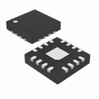
MAX4674ETE+ Maxim Integrated Products, MAX4674ETE+ Datasheet - Page 4

MAX4674ETE+
Manufacturer Part Number
MAX4674ETE+
Description
IC MULTIPLEXER QUAD 2X1 16TQFN
Manufacturer
Maxim Integrated Products
Datasheet
1.MAX4674ESE.pdf
(13 pages)
Specifications of MAX4674ETE+
Function
Multiplexer
Circuit
4 x 2:1
On-state Resistance
4 Ohm
Voltage Supply Source
Single Supply
Voltage - Supply, Single/dual (±)
1.8 V ~ 5.5 V
Current - Supply
1µA
Operating Temperature
-40°C ~ 85°C
Mounting Type
Surface Mount
Package / Case
16-TQFN Exposed Pad
Lead Free Status / RoHS Status
Lead free / RoHS Compliant
3V/5V, 4Ω, Wideband Quad
2:1 Analog Multiplexer
4
Note 2: The algebraic convention, where the most negative value is a minimum and the most positive value a maximum, is used in
Note 3: Parts are tested at the maximum hot-rated temperature. Limits across the entire temperature range are guaranteed by
Note 4: ∆R
Note 5: ∆R
Note 6: Flatness is defined as the difference between the maximum and minimum value of on-resistance as measured over the
Note 7: Guaranteed by design.
Note 8: Off-Isolation = 20log
Note 9: Between any two switches.
ELECTRICAL CHARACTERISTICS—Single +3V Supply (continued)
(V+ = +2.7V to +3.3V, V
COM_ Off-Leakage Current
(Note 7)
COM_ On-Leakage Current
(Note 7)
DIGITAL I/O (A0, EN)
Input Logic High
Input Logic Low
Input Leakage Current
DYNAMIC
Turn-On Time (Note 7)
Turn-Off Time (Note 7)
Break-Before-Make (Note 7)
Charge Injection
Off-Isolation (Note 8)
Crosstalk (Note 9)
NO_, NC_ Off-Capacitance
COM_ Off-Capacitance
COM_ On-Capacitance
SUPPLY
Positive Supply Current
_______________________________________________________________________________________
this data sheet.
design and correlation.
specified analog signal range.
PARAMETER
ON
ON
= R
matching specifications for QFN packaged parts are guaranteed by design.
ON(MAX)
IH
= 2.0V, V
- R
10
ON(MIN)
(V
C
COM
I
C
C
I
COM_(OFF)
SYMBOL
COM_(ON)
COM_(OFF)
NO_(OFF)
NC_(OFF)
IL
C
t
V
t
V
t
BBM
V
I
V
OFF
.
= 0.4V, T
I+
ON
(ON)
IN
/V
Q
ISO
CT
IH
IL
NO
), V
,
COM
A
V + = 3.3V ; V
V
V + = 3.3V ; V
V
floating
V
R
Figure 2
V
R
Figure 2
V
R
Figure 3
C
f = 10MHz, Figure 5
C
f = 10MHz, Figure 5
V+ = 3.3V, V
V
V
Figure 4
V
V
V
Figure 6
=T
N O_
NO_
NO_
NO_
NO_
L
L
L
L
L
IN
GEN
NO_
COM_
COM_
= 100Ω, C
= 100Ω, C
= 100Ω, C
= 5pF, R
= 5pF, R
= output, V
MIN
= 0 or +5.5V
or V
or V
or V
or V
or V
or V
= 2V, R
to T
= GND, f = 1MHz, Figure 6
= V
N C _
NC_
NC_
NC_
NC
NC_
NO_
MAX
L
L
C OM _
C OM _
IN
= 1.5V,
= 100Ω,
= 100Ω,
= 3V , 1V
= 1V, 3V, or
L
L
L
GEN
= 1.5V,
= 1.5V,
= GND, f = 1MHz, Figure 6
NO
, V
= 0 or V+
= 35pF,
= 35pF,
= 35pF,
, unless otherwise noted. Typical values at T
CONDITIONS
NC_
= 1V , 3V ;
= 1V , 3V ;
= input to off switch.
= 0, C
= GND, f = 1MHz,
L
= 1.0nF,
T
T
T
T
T
T
T
T
T
T
T
T
T
T
T
f = 10MHz
f = 1MHz
f = 10MHz
f = 1MHz
A
A
MAX
A
A
MAX
A
A
MAX
A
A
MAX
A
A
MAX
= +25°C
= T
= +25°C
= T
= +25°C
= T
= +25°C
= T
= +25°C
= T
MIN
MIN
MIN
MIN
MIN
to
to
to
to
to
MIN
-0.5
-0.5
-0.5
2.0
-1
-1
1
±0.01
±0.01
0.001
-114
TYP
A
-47
-67
-68
±1
12
18
10
20
30
5
5
= +25°C.) (Notes 2, 3)
MAX
+0.5
+0.5
+0.5
0.4
1.0
+1
+1
22
25
10
8
UNITS
pC
dB
dB
nA
nA
µA
pF
pF
pF
µA
ns
ns
ns
V
V


