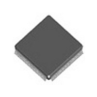
ADSP-21266SKSTZ-2C Analog Devices Inc, ADSP-21266SKSTZ-2C Datasheet - Page 32

ADSP-21266SKSTZ-2C
Manufacturer Part Number
ADSP-21266SKSTZ-2C
Description
Manufacturer
Analog Devices Inc
Datasheet
1.ADSP-21266SKSTZ-2C.pdf
(44 pages)
Specifications of ADSP-21266SKSTZ-2C
Device Core Size
32b
Architecture
Super Harvard
Format
Floating Point
Clock Freq (max)
200MHz
Mips
200
Device Input Clock Speed
200MHz
Ram Size
256KB
Program Memory Size
512KB
Operating Supply Voltage (typ)
1.2/3.3V
Operating Supply Voltage (min)
1.14/3.13V
Operating Supply Voltage (max)
1.26/3.47V
Operating Temp Range
0C to 70C
Operating Temperature Classification
Commercial
Mounting
Surface Mount
Pin Count
144
Package Type
LQFP
Lead Free Status / Rohs Status
Compliant
Available stocks
Company
Part Number
Manufacturer
Quantity
Price
Company:
Part Number:
ADSP-21266SKSTZ-2C
Manufacturer:
AD
Quantity:
50
Part Number:
ADSP-21266SKSTZ-2C
Manufacturer:
ADI/亚德诺
Quantity:
20 000
ADSP-21261/ADSP-21262/ADSP-21266
Parallel Data Acquisition Port (PDAP)
The timing requirements for the PDAP are provided in
and
Channel 0 of the IDP. For details on the operation of the IDP,
see the IDP chapter of the ADSP-2126x Peripherals Manual.
Table 34. Parallel Data Acquisition Port (PDAP)
1
Parameter
Timing Requirements
t
t
t
t
t
t
Switching Characteristics
t
t
Source pins of DATA are ADDR7–0, DATA7–0, or DAI pins. Source pins for SCLK and FS are: 1) DAI pins, 2) CLKIN through PCG, or 3) DAI pins through PCG.
SPCLKEN
HPCLKEN
PDSD
PDHD
PDCLKW
PDCLK
PDHLDD
PDSTRB
Figure
23. PDAP is the parallel mode operation of
PDAP_CLKEN Setup Before PDAP_CLK Sample Edge
PDAP_CLKEN Hold After PDAP_CLK Sample Edge
PDAP_DAT Setup Before SCLK PDAP_CLK Sample Edge
PDAP_DAT Hold After SCLK PDAP_CLK Sample Edge
Clock Width
Clock Period
Delay of PDAP Strobe After Last PDAP_CLK Capture Edge for a Word
PDAP Strobe Pulse Width
(PDAP_STROBE)
(PDAP_CLKEN)
(PDAP_CLK)
DAI_P20–1
DAI_P20–1
DAI_P20–1
DATA
Figure 23. Parallel Data Acquisition Port (PDAP)
Rev. F | Page 32 of 44 | July 2009
Table 34
t
PDCLKW
SAMPLE EDGE
t
SPCLKEN
t
PDSD
1
t
PDHLDD
1
1
Note that the most significant 16 bits of external PDAP data can
be provided through either the parallel port AD15–0 or the
DAI_P20–5 pins. The remaining four bits can only be sourced
through DAI_P4–1. The timing below is valid at the
DAI_P20–1 pins or at the AD15–0 pins.
1
t
PDCLK
t
HPCLKEN
t
PDHD
t
PDSTRB
Min
2.5
2.5
2.5
2.5
7
20
2 × t
1 × t
CCLK
CCLK
– 1
Max
Unit
ns
ns
ns
ns
ns
ns
ns
ns


