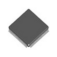
ADSP-21266SKSTZ-2C Analog Devices Inc, ADSP-21266SKSTZ-2C Datasheet - Page 17

ADSP-21266SKSTZ-2C
Manufacturer Part Number
ADSP-21266SKSTZ-2C
Description
Manufacturer
Analog Devices Inc
Datasheet
1.ADSP-21266SKSTZ-2C.pdf
(44 pages)
Specifications of ADSP-21266SKSTZ-2C
Device Core Size
32b
Architecture
Super Harvard
Format
Floating Point
Clock Freq (max)
200MHz
Mips
200
Device Input Clock Speed
200MHz
Ram Size
256KB
Program Memory Size
512KB
Operating Supply Voltage (typ)
1.2/3.3V
Operating Supply Voltage (min)
1.14/3.13V
Operating Supply Voltage (max)
1.26/3.47V
Operating Temp Range
0C to 70C
Operating Temperature Classification
Commercial
Mounting
Surface Mount
Pin Count
144
Package Type
LQFP
Lead Free Status / Rohs Status
Compliant
Available stocks
Company
Part Number
Manufacturer
Quantity
Price
Company:
Part Number:
ADSP-21266SKSTZ-2C
Manufacturer:
AD
Quantity:
50
Part Number:
ADSP-21266SKSTZ-2C
Manufacturer:
ADI/亚德诺
Quantity:
20 000
Power-Up Sequencing
The timing requirements for DSP startup are given in
and
approximately 200 A may be observed on the RESET pin. This
leakage current results from the weak internal pull-up resistor
on this pin being enabled during power-up.
Table 15. Power-Up Sequencing (DSP Startup)
1
2
3
4
5
Parameter
Timing Requirements
t
t
t
t
t
Switching Characteristics
t
Valid V
Assumes a stable CLKIN signal, after meeting worst-case startup timing of crystal oscillators. Refer to the crystal oscillator manufacturer’s data sheet for startup time.
Based on CLKIN cycles.
Applies after the power-up sequence is complete. Subsequent resets require a minimum of four CLKIN cycles for RESET to be held low in order to properly initialize and
The 4096 cycle count depends on t
RSTVDD
IVDDEVDD
CLKVDD
CLKRST
PLLRST
CORERST
depending on the design of the power supply subsystem.
Assume a 25 ms maximum oscillator startup time if using the XTAL pin and internal oscillator circuit in conjunction with an external crystal.
propagate default states at all I/O pins.
4097 cycles maximum.
Figure
DDINT
5. Note that during power-up, a leakage current of
/V
(MULTIPLEXED WITH CLKOUT)
DDEXT
assumes that the supplies are fully ramped to their 1.2 V and 3.3 V rails. Voltage ramp rates can vary from microseconds to hundreds of milliseconds
RESETOUT
RESET Low Before V
V
CLKIN Valid After V
CLKIN Valid Before RESET Deasserted
PLL Control Setup Before RESET Deasserted
DSP Core Reset Deasserted After RESET Deasserted
DDINT
CLK_CFG1–0
SRST
On Before V
V
RESET
V
specification in
CLKIN
DDEXT
DDINT
DDEXT
DDINT
DDINT
Table
/V
/V
t
RSTVDD
DDEXT
DDEXT
17. If setup time is not met, one additional CLKIN cycle can be added to the core reset time, resulting in
Valid
Rev. F | Page 17 of 44 | July 2009
On
Figure 5. Power-Up Sequencing
Table 15
1
t
IVDDEVDD
t
PLLRST
ADSP-21261/ADSP-21262/ADSP-21266
t
t
CLKVDD
CLKRST
Min
0
–50
0
10
20
4096 t
2
3
CK
t
CORERST
4, 5
Max
+200
200
Unit
ns
ms
ms
μs
μs


