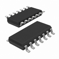
74HCT4016D,112 NXP Semiconductors, 74HCT4016D,112 Datasheet - Page 2

74HCT4016D,112
Manufacturer Part Number
74HCT4016D,112
Description
IC SWITCH QUAD SPST 14SOIC
Manufacturer
NXP Semiconductors
Series
74HCTr
Datasheets
1.74HCT4046ADB112.pdf
(19 pages)
2.74HCT4046ADB112.pdf
(23 pages)
3.74HCT4016N112.pdf
(14 pages)
Specifications of 74HCT4016D,112
Package / Case
14-SOIC (0.154", 3.90mm Width)
Function
Switch
Circuit
4 x SPST - NO
On-state Resistance
80 Ohm
Voltage Supply Source
Single Supply
Voltage - Supply, Single/dual (±)
4.5 V ~ 5.5 V
Current - Supply
2µA
Mounting Type
Surface Mount
Switch Configuration
SPST
On Resistance (max)
320 Ohm @ 4.5 V
On Time (max)
35 ns @ 4.5 V
Off Time (max)
35 ns @ 4.5 V
Supply Voltage (max)
5.5 V
Supply Voltage (min)
4.5 V
Maximum Power Dissipation
500 mW
Maximum Operating Temperature
+ 125 C
Mounting Style
SMD/SMT
Minimum Operating Temperature
- 40 C
Lead Free Status / RoHS Status
Lead free / RoHS Compliant
Lead Free Status / RoHS Status
Lead free / RoHS Compliant, Lead free / RoHS Compliant
Other names
568-2844-5
933714390112
933714390112
Philips Semiconductors
FEATURES
GENERAL DESCRIPTION
The 74HC/HCT4016 are high-speed Si-gate CMOS
devices and are pin compatible with the “4016” of the
QUICK REFERENCE DATA
GND = 0 V; T
Notes
1. C
2. For HC the condition is V
ORDERING INFORMATION
See
December 1990
t
t
C
C
C
PZH
PHZ
Low “ON” resistance:
160
120
80
Individual switch controls
Typical “break before make” built in
Output capability: non-standard
I
Quad bilateral switches
I
PD
S
CC
f
f
C
C
V
For HCT the condition is V
SYMBOL
i
o
“74HC/HCT/HCU/HCMOS Logic Package Information”
/ t
/ t
CC
PD
= input frequency in MHz
L
S
category: SSI
= output frequency in MHz
{(C
PZL
PLZ
= output load capacitance in pF
P
= max. switch capacitance in pF
= supply voltage in V
is used to determine the dynamic power dissipation (P
D
(typ.) at V
(typ.) at V
(typ.) at V
L
= C
C
amb
S
PD
)
= 25 C; t
V
CC
CC
CC
V
turn “ON” time E
turn “OFF” time E
input capacitance
power dissipation capacitance per switch
max. switch capacitance
CC
CC
= 4.5 V
= 6.0 V
= 9.0 V
2
2
f
f
o
r
i
} = sum of outputs
= t
I
I
f
= GND to V
= GND to V
= 6 ns
{ (C
PARAMETER
L
n
n
to V
to V
C
S
OS
)
OS
CC
CC
V
CC
1.5 V
2
f
o
} where:
2
.
“4000B” series. They are specified in compliance with
JEDEC standard no. 7A.
The 74HC/HCT4016 have four independent analog
switches (transmission gates).
Each switch has two input/output terminals (Y
active HIGH enable input (E
V
established (ON condition). When E
ground (GND), the switch is disabled and a high
impedance between Y
condition).
Current through a switch will not cause additional
V
switch is maintained within the supply voltage range;
V
equivalent terminals.
CC
CC
CC
D
in W):
, a low bidirectional path between Y
C
V
notes 1 and 2
current provided the voltage at the terminals of the
>> (V
CC
L
= 15 pF; R
= 5 V
CONDITIONS
Y
, V
Z
) >> GND. Inputs Y
L
= 1 k ;
n
and Z
n
). When E
n
16
14
3.5
12
5
74HC/HCT4016
is established (OFF
HC
TYPICAL
n
Product specification
and Z
n
is connected to
17
20
3.5
12
5
n
n
HCT
is connected to
and Z
n
are electrically
n
, Z
n
n
is
ns
ns
pF
pF
pF
) and an
UNIT


