74HCT4016N,112 NXP Semiconductors, 74HCT4016N,112 Datasheet - Page 10
74HCT4016N,112
Manufacturer Part Number
74HCT4016N,112
Description
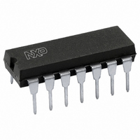
IC SWITCH QUAD SPST 14DIP
Manufacturer
NXP Semiconductors
Series
74HCTr
Datasheets
1.74HCT4046ADB112.pdf
(19 pages)
2.74HCT4046ADB112.pdf
(23 pages)
3.74HCT4016N112.pdf
(14 pages)
Specifications of 74HCT4016N,112
Package / Case
14-DIP (0.300", 7.62mm)
Function
Switch
Circuit
4 x SPST - NO
On-state Resistance
80 Ohm
Voltage Supply Source
Single Supply
Voltage - Supply, Single/dual (±)
4.5 V ~ 5.5 V
Current - Supply
2µA
Mounting Type
Through Hole
Switch Configuration
SPST
On Resistance (max)
320 Ohm @ 4.5 V
On Time (max)
35 ns @ 4.5 V
Off Time (max)
35 ns @ 4.5 V
Supply Voltage (max)
5.5 V
Supply Voltage (min)
4.5 V
Maximum Power Dissipation
750 mW
Maximum Operating Temperature
+ 125 C
Mounting Style
Through Hole
Minimum Operating Temperature
- 40 C
Lead Free Status / RoHS Status
Lead free / RoHS Compliant
Lead Free Status / RoHS Status
Lead free / RoHS Compliant, Lead free / RoHS Compliant
Other names
568-2845-5
933668980112
933668980112


Philips Semiconductors
AC CHARACTERISTICS FOR 74HCT
GND = 0 V; t
ADDITIONAL AC CHARACTERISTICS FOR 74HC/HCT
Recommended conditions and typical values
GND = 0 V; t
Notes
1. V
2. V
3. Adjust input voltage V
4. Adjust input voltage V
December 1990
SYMBOL PARAMETER
t
t
t
t
SYMBOL
V
f
C
PHL
PZH
PZL
PHZ
max
(p-p)
Quad bilateral switches
S
/ t
/ t
is
os
PLH
PLZ
is the input voltage at a Y
is the output voltage at a Y
propagation delay
turn “ON” time
turn “ON” time
turn “OFF” time
r
r
V
E
E
E
= t
= t
PARAMETER
sine-wave distortion
sine-wave distortion
switch “OFF” signal
crosstalk between
crosstalk voltage between
minimum frequency response
maximum switch capacitance
is
n
n
n
f = 1 kHz
f = 10 kHz
feed-through
any two switches
enable or address input
to any switch
(peak-to-peak value)
( 3dB)
f
to V
to V
to V
f
to V
= 6 ns; C
= 6 ns
os
os
os
os
is
is
L
to 0 dBm level (0 dBm = 1 mW into 600 ).
to 0 dBm level at V
= 50 pF
n
min. typ. max. min. max. min. max.
or Z
n
or Z
n
6
19
20
23
terminal, whichever is assigned as an input.
n
25
terminal, whichever is assigned as an output.
12
35
35
35
typ.
0.80
0.40
2.40
1.20
110
220
150
160
5
os
50
50
60
60
for 1 MHz (0 dBm = 1 mW into 50 ).
T
74HCT
amb
40 to 85
UNIT
%
%
%
%
dB
dB
dB
dB
mV
mV
MHz
MHz
pF
( C)
10
15
44
44
44
4.5
9.0
4.5
9.0
4.5
9.0
4.5
9.0
4.5
9.0
4.5
9.0
V
(V)
40 to 125
CC
18
53
53
53
4.0
8.0
4.0
8.0
note 3
note 3
note 4
V
is(p-p)
(V)
UNIT
ns
ns
ns
ns
CONDITIONS
R
(see Fig.14)
R
(see Fig.14)
R
f = 1 MHz (see Figs 10 and 15)
R
f = 1 MHz (see Fig.12)
R
f = 1 MHz (E
between V
t
R
(see Figs 11 and 14)
r
L
L
L
L
L
L
= t
= 10 k ; C
= 10 k ; C
= 600 ; C
= 600 ; C
= 600 ; C
= 50 ; C
4.5
4.5
4.5
4.5
V
(V)
f
CC
= 6 ns) (see Fig.13)
74HC/HCT4016
TEST CONDITIONS
OTHER
R
(see Fig.16)
R
(see Figs 17 and 18)
R
(see Figs 17 and 18)
R
(see Figs 17 and 18)
L
L
L
L
CC
Product specification
= ; C
= 1 k ; C
= 1 k ; C
= 1 k ; C
n
L
, square wave
and GND,
L
L
L
L
L
= 10 pF
= 50 pF
= 50 pF
= 50 pF;
= 50 pF;
= 50 pF;
L
= 50 pF
L
L
L
= 50 pF
= 50 pF
= 50 pF
Related parts for 74HCT4016N,112
Image
Part Number
Description
Manufacturer
Datasheet
Request
R

Part Number:
Description:
NXP Semiconductors designed the LPC2420/2460 microcontroller around a 16-bit/32-bitARM7TDMI-S CPU core with real-time debug interfaces that include both JTAG andembedded trace
Manufacturer:
NXP Semiconductors
Datasheet:

Part Number:
Description:
NXP Semiconductors designed the LPC2458 microcontroller around a 16-bit/32-bitARM7TDMI-S CPU core with real-time debug interfaces that include both JTAG andembedded trace
Manufacturer:
NXP Semiconductors
Datasheet:
Part Number:
Description:
NXP Semiconductors designed the LPC2468 microcontroller around a 16-bit/32-bitARM7TDMI-S CPU core with real-time debug interfaces that include both JTAG andembedded trace
Manufacturer:
NXP Semiconductors
Datasheet:
Part Number:
Description:
NXP Semiconductors designed the LPC2470 microcontroller, powered by theARM7TDMI-S core, to be a highly integrated microcontroller for a wide range ofapplications that require advanced communications and high quality graphic displays
Manufacturer:
NXP Semiconductors
Datasheet:
Part Number:
Description:
NXP Semiconductors designed the LPC2478 microcontroller, powered by theARM7TDMI-S core, to be a highly integrated microcontroller for a wide range ofapplications that require advanced communications and high quality graphic displays
Manufacturer:
NXP Semiconductors
Datasheet:
Part Number:
Description:
The Philips Semiconductors XA (eXtended Architecture) family of 16-bit single-chip microcontrollers is powerful enough to easily handle the requirements of high performance embedded applications, yet inexpensive enough to compete in the market for hi
Manufacturer:
NXP Semiconductors
Datasheet:
Part Number:
Description:
The XA-S3 device is a member of Philips Semiconductors? XA(eXtended Architecture) family of high performance 16-bitsingle-chip microcontrollers
Manufacturer:
NXP Semiconductors
Datasheet:

Part Number:
Description:
The NXP BlueStreak LH75401/LH75411 family consists of two low-cost 16/32-bit System-on-Chip (SoC) devices
Manufacturer:
NXP Semiconductors
Datasheet:
Part Number:
Description:
The NXP LPC3130/3131 combine an 180 MHz ARM926EJ-S CPU core, high-speed USB2
Manufacturer:
NXP Semiconductors
Datasheet:
Part Number:
Description:
The NXP LPC3141 combine a 270 MHz ARM926EJ-S CPU core, High-speed USB 2
Manufacturer:
NXP Semiconductors
Part Number:
Description:
The NXP LPC3143 combine a 270 MHz ARM926EJ-S CPU core, High-speed USB 2
Manufacturer:
NXP Semiconductors

Part Number:
Description:
The NXP LPC3152 combines an 180 MHz ARM926EJ-S CPU core, High-speed USB 2
Manufacturer:
NXP Semiconductors
Part Number:
Description:
The NXP LPC3154 combines an 180 MHz ARM926EJ-S CPU core, High-speed USB 2
Manufacturer:
NXP Semiconductors

Part Number:
Description:
Standard level N-channel enhancement mode Field-Effect Transistor (FET) in a plastic package using NXP High-Performance Automotive (HPA) TrenchMOS technology
Manufacturer:
NXP Semiconductors
Datasheet: