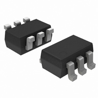
NLASB3157DFT2G ON Semiconductor, NLASB3157DFT2G Datasheet - Page 2

NLASB3157DFT2G
Manufacturer Part Number
NLASB3157DFT2G
Description
IC SWITCH SPDT SC88
Manufacturer
ON Semiconductor
Type
Analog Switchr
Datasheet
1.NLASB3157DFT2G.pdf
(10 pages)
Specifications of NLASB3157DFT2G
Function
Switch
Circuit
1 x SPDT
On-state Resistance
7 Ohm
Voltage Supply Source
Single Supply
Voltage - Supply, Single/dual (±)
1.65 V ~ 5.5 V
Current - Supply
1µA
Operating Temperature
-55°C ~ 125°C
Mounting Type
Surface Mount
Package / Case
6-TSSOP, SC-88, SOT-363
Multiplexer Configuration
Single SPDT
Number Of Inputs
1
Number Of Outputs
2
Number Of Channels
1
Analog Switch On Resistance
50@1.65VOhm
Analog Switch Turn On Time
23ns
Analog Switch Turn Off Time
12.5ns
Package Type
SOT-363
Power Supply Requirement
Single
Single Supply Voltage (min)
1.65V
Single Supply Voltage (typ)
3/5V
Single Supply Voltage (max)
5.5V
Dual Supply Voltage (min)
Not RequiredV
Dual Supply Voltage (typ)
Not RequiredV
Dual Supply Voltage (max)
Not RequiredV
Power Dissipation
180mW
Mounting
Surface Mount
Pin Count
6
Operating Temp Range
-55C to 125C
Operating Temperature Classification
Military
Lead Free Status / RoHS Status
Lead free / RoHS Compliant
Other names
NLASB3157DFT2GOSTR
Available stocks
Company
Part Number
Manufacturer
Quantity
Price
Company:
Part Number:
NLASB3157DFT2G
Manufacturer:
ON
Quantity:
6 000
Part Number:
NLASB3157DFT2G
Manufacturer:
ON/安森美
Quantity:
20 000
Stresses exceeding Maximum Ratings may damage the device. Maximum Ratings are stress ratings only. Functional operation above the
Recommended Operating Conditions is not implied. Extended exposure to stresses above the Recommended Operating Conditions may affect
device reliability.
1. The input and output negative voltage ratings may be exceeded if the input and output diode current ratings are observed.
2. Select input must be held HIGH or LOW, it must not float.
MAXIMUM RATINGS
RECOMMENDED OPERATING CONDITIONS
Supply Voltage
DC Switch Voltage (Note 1)
DC Input Voltage (Note 1)
DC Input Diode Current @ V
DC Output Current
DC V
Storage Temperature Range
Junction Temperature Under Bias
Junction Lead Temperature (Soldering, 10 Seconds)
Power Dissipation @ +85°C
Supply Voltage Operating
Select Input Voltage
Switch Input Voltage
Output Voltage
Operating Temperature
Input Rise and Fall Time
Thermal Resistance
Control Input V
Control Input V
CC
or Ground Current
GND
CC
CC
B
B
= 2.3 V−3.6 V
= 4.5 V−5.5 V
1
0
1
2
3
IN
t 0 V
Characteristic
Rating
(Top View)
SC−88
Figure 1. Pin Assignment & Logic Diagram
(Note 2)
6
5
4
http://onsemi.com
Select
V
A
CC
2
I
Symbol
Symbol
GND
CC
V
I
V
V
T
V
V
V
V
t
q
OUT
B
B
P
I
T
T
OUT
T
/I
r
stg
, t
CC
IK
CC
JA
IS
IN
IN
IS
A
1
0
GND
J
L
D
f
1
2
3
(Top View)
WDFN6
−0.5 to V
1.65
Min
−55
0
0
0
0
0
−
−0.5 to + 7.0
−0.5 to +7.0
−65 to +150
6
5
4
Value
+100
−50
128
150
260
180
Select
V
A
CC
CC
+125
+ 0.5
Max
V
V
350
5.5
5.5
5.0
10
CC
CC
°C/W
Unit
Unit
ns/V
mW
mA
mA
mA
°C
°C
°C
°C
V
V
V
V
V
V
V


