MC74VHC1G66DTT1G ON Semiconductor, MC74VHC1G66DTT1G Datasheet
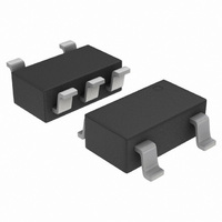
IC SWITCH SPST SOT23-5

MC74VHC1G66DTT1G

Manufacturer Part Number
MC74VHC1G66DTT1G
Description
IC SWITCH SPST SOT23-5
Manufacturer
ON Semiconductor
Series
74VHCr
Type
Analog Switchr
Datasheet

Specifications of MC74VHC1G66DTT1G

Function
Switch
Circuit
1 x SPST- NO
On-state Resistance
40 Ohm
Voltage Supply Source
Single Supply
Voltage - Supply, Single/dual (±)
2 V ~ 5.5 V
Current - Supply
1µA
Operating Temperature
-55°C ~ 125°C
Mounting Type
Surface Mount
Package / Case
TSOT-23-5, TSOT-5, TSOP-5
Switch Configuration
SPST
On Resistance (max)
60 Ohms
On Time (max)
40 ns
Off Time (max)
40 ns
Supply Voltage (max)
5.5 V
Supply Voltage (min)
2 V
Maximum Power Dissipation
200 mW
Maximum Operating Temperature
+ 125 C
Mounting Style
SMD/SMT
Minimum Operating Temperature
- 55 C
Propagation Delay Time
5 ns
Multiplexer Configuration
Single SPST
Number Of Inputs
1
Number Of Outputs
1
Number Of Channels
1
Analog Switch On Resistance
60@3VOhm
Analog Switch Turn On Time
40ns
Analog Switch Turn Off Time
40ns
Package Type
TSOP
Power Supply Requirement
Single
Single Supply Voltage (min)
2V
Single Supply Voltage (typ)
3/5V
Single Supply Voltage (max)
5.5V
Dual Supply Voltage (min)
Not RequiredV
Dual Supply Voltage (typ)
Not RequiredV
Dual Supply Voltage (max)
Not RequiredV
Power Dissipation
200mW
Mounting
Surface Mount
Pin Count
5
Operating Temp Range
-55C to 125C
Operating Temperature Classification
Military
Lead Free Status / RoHS Status
Lead free / RoHS Compliant
Other names
MC74VHC1G66DTT1GOS
MC74VHC1G66DTT1GOS
MC74VHC1G66DTT1GOSTR

Available stocks

Company
Part Number
Manufacturer
Quantity
Price
Part Number:
MC74VHC1G66DTT1G
Manufacturer:
ON Semiconductor
Quantity:
53 820
Part Number:
MC74VHC1G66DTT1G
Manufacturer:
ON Semiconductor
Quantity:
9 800
MC74VHC1G66,
NLVHC1G66
SPST (NO) Normally Open
Analog Switch
(SPST) analog switch. It achieves high speed propagation delays and
low ON resistances while maintaining low power dissipation. This
bilateral switch controls analog and digital voltages that may vary
across the full power−supply range (from V
single gate of the High Speed CMOS MC74VHC4066 and the
metal−gate CMOS MC14066. The device has been designed so that
the ON resistances (R
voltage than R
analog switches.
1.2x1.0x0.55mm UDFN6 package.
outputs. The ON/OFF control input structure provides protection when
voltages between 0 V and 5.5 V are applied, regardless of the supply
voltage. This input structure helps prevent device destruction caused by
supply voltage − input/output voltage mismatch, battery backup,
hot insertion, etc.
Features
© Semiconductor Components Industries, LLC, 2007
February, 2007 − Rev. 13
The MC74VHC1G66, NLVHC1G66 is a single pole single throw
The MC74VHC1G66, NLVHC1G66 is compatible in function to a
The newer NLVHC offers the same functionality in a
The ON/OFF control inputs are compatible with standard CMOS
High Speed: t
Low Power Dissipation: I
Diode Protection Provided on Inputs and Outputs
Improved Linearity and Lower ON Resistance over Input Voltage
Chip Complexity: 11 FETs or 3 Equivalent Gates
ON/OFF Control Input has OVT
Chip Complexity: FETs = 11
Pb−Free Packages are Available
ON
PD
of the metal−gate CMOS or High Speed CMOS
= 20 ns (Typ) at V
ON
) are much lower and more linear over input
CC
= 1.0 mA (Max) at T
CC
= 5.0 V
CC
to GND).
A
= 25°C
1
See detailed ordering and shipping information in the package
dimensions section on page 7 of this data sheet.
On/Off Control Input
CASE 517AA
*Date Code orientation and/or position may
CASE 419A
MU SUFFIX
DF SUFFIX
DT SUFFIX
CASE 483
vary depending upon manufacturing location.
5
(Note: Microdot may be in either location)
SC−88A
TSOP−5
UDFN6
1
2
4
3
5
1
ORDERING INFORMATION
1
V9, V
M
W
G
H
L
http://onsemi.com
FUNCTION TABLE
PIN ASSIGNMENT
= Device Code
= Date Code*
= Work Week
= Pb−Free Package
ON/OFF CONTROL
MARKING DIAGRAMS
Publication Order Number:
State of Analog Switch
IN/OUT X
OUT/IN Y
5
1
GND
5
1
V
CC
MC74VHC1G66/D
V9 M G
VW M
V9 M G
G
A
A
Off
On
G
G

Related parts for MC74VHC1G66DTT1G

MC74VHC1G66DTT1G Summary of contents

Page 1

MC74VHC1G66, NLVHC1G66 SPST (NO) Normally Open Analog Switch The MC74VHC1G66, NLVHC1G66 is a single pole single throw (SPST) analog switch. It achieves high speed propagation delays and low ON resistances while maintaining low power dissipation. This bilateral switch controls analog ...

Page 2

IN/OUT OUT/ GND 3 (SC−88A, TSOP−5) ON/OFF CONTROL IN/OUT X MAXIMUM RATINGS Symbol V DC Supply Voltage CC V Digital Input Voltage IN V Analog Output Voltage IS I Digital Input Diode Current IK ...

Page 3

RECOMMENDED OPERATING CONDITIONS Symbol Characteristics V DC Supply Voltage Input Voltage Output Voltage IS T Operating Temperature Range Input Rise and Fall Time r f ON/OFF Control Input Device Junction ...

Page 4

AC ELECTRICAL CHARACTERISTICS Î Î Î Î ...

Page 5

PLOTTER POWER DC PARAMETER SUPPLY COMPUTER − Figure 4. On Resistance Test Set− N Figure 6. Maximum On−Channel Leakage Current Test Set−Up Switch to Position 2 ...

Page 6

Meter *Includes all probe and jig capacitance. Figure 10. Maximum On−Channel Bandwidth Test Set− Figure 12. Feedthrough Noise, ON/OFF Control to To Distortion Meter V OS ...

Page 7

... Analog Out Figure 15. Propagation Delay, ON/OFF Control ORDERING INFORMATION Device MC74VHC1G66DFT1 MC74VHC1G66DFT1G MC74VHC1G66DFT2 MC74VHC1G66DFT2G MC74VHC1G66DTT1 MC74VHC1G66DTT1G NLVHC1G66MUR2G †For information on tape and reel specifications, including part orientation and tape sizes, please refer to our Tape and Reel Packaging Specifications Brochure, BRD8011/D. MC74VHC1G66, NLVHC1G66 ...

Page 8

... H SOLDERING FOOTPRINT* 0.50 0.0197 0.40 0.0157 *For additional information on our Pb−Free strategy and soldering details, please download the ON Semiconductor Soldering and Mounting Techniques Reference Manual, SOLDERRM/D. SC−88A, SOT−353, SC−70 CASE 419A−02 ISSUE J NOTES: 1. DIMENSIONING AND TOLERANCING PER ANSI Y14.5M, 1982. ...

Page 9

... A C SEATING 0.05 PLANE H T *For additional information on our Pb−Free strategy and soldering details, please download the ON Semiconductor Soldering and Mounting Techniques Reference Manual, SOLDERRM/D. PACKAGE DIMENSIONS TSOP−5, SOT23−5 CASE 483−02 ISSUE F NOTES: 1. DIMENSIONING AND TOLERANCING PER 2. CONTROLLING DIMENSION: MILLIMETERS. ...

Page 10

... PITCH *For additional information on our Pb−Free strategy and soldering details, please download the ON Semiconductor Soldering and Mounting Techniques Reference Manual, SOLDERRM/D. N. American Technical Support: 800−282−9855 Toll Free USA/Canada Europe, Middle East and Africa Technical Support: Phone: 421 33 790 2910 Japan Customer Focus Center Phone: 81− ...

Related keywords