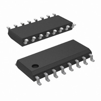
DS90CP22M-8/NOPB National Semiconductor, DS90CP22M-8/NOPB Datasheet - Page 3

DS90CP22M-8/NOPB
Manufacturer Part Number
DS90CP22M-8/NOPB
Description
IC CROSSPOINT SWITCH 2X2 16SOIC
Manufacturer
National Semiconductor
Datasheet
1.DS90CP22M-8NOPB.pdf
(10 pages)
Specifications of DS90CP22M-8/NOPB
Function
Crosspoint Switch
Circuit
1 x 2:2
Voltage Supply Source
Single Supply
Voltage - Supply, Single/dual (±)
3 V ~ 3.6 V
Current - Supply
98mA
Operating Temperature
-40°C ~ 85°C
Mounting Type
Surface Mount
Package / Case
16-SOIC (0.154", 3.90mm Width)
For Use With
LVDSCP22EVK - EVALUATION BOARD FOR DS90CP22
Lead Free Status / RoHS Status
Lead free / RoHS Compliant
Other names
*DS90CP22M-8
*DS90CP22M-8/NOPB
DS90CP22M-8
*DS90CP22M-8/NOPB
DS90CP22M-8
Available stocks
Company
Part Number
Manufacturer
Quantity
Price
Company:
Part Number:
DS90CP22M-8/NOPB
Manufacturer:
NS
Quantity:
90
T
T
T
T
T
T
T
T
T
T
T
T
T
T
SET
HOLD
SWITCH
PHZ
PLZ
PZH
PZL
LHT
HLT
JIT
PLHD
PHLD
SKEW
CCS
Symbol
AC Electrical Characteristics
Over recommended operating supply and temperature ranges unless otherwise specified (Note 4)
Note 4: The parameters are guaranteed by design. The limits are based on statistical analysis of the device performance over PVT (process, voltage and
temperature) range.
Note 5: T
Note 6: The parameters are guaranteed by design. The limits are based on statistical analysis of the device performance over PVT range with the following
equipment test setup: HP70004A (display mainframe) with HP70841B (pattern generator), 5 feet of RG-142 cable with DUT test board and HP83480A (digital
scope mainframe) with HP83483A (20GHz scope module).
SET
Input to SEL Setup Time, Figures 1, 2
(Note 5)
Input to SEL Hold Time, Figures 1, 2
(Note 5)
SEL to Switched Output, Figures 1, 2
Disable Time (Active to TRI-STATE) High to Z, Figure 3
Disable Time (Active to TRI-STATE) Low to Z, Figure 3
Enable Time (TRI-STATE to Active) Z to High, Figure 3
Enable Time (TRI-STATE to Active) Z to Low, Figure 3
Output Low-to-High Transition Time, 20% to 80%, Figure 5
Output High-to-Low Transition Time, 80% to 20%, Figure 5
LVDS Data Path Peak to Peak Jitter, (Note
6)
Propagation Low to High Delay, Figure 6
Propagation Low to High Delay, Figure 6
Propagation High to Low Delay, Figure 6
Propagation High to Low Delay, Figure 6
Pulse Skew |T
Output Channel-to-Channel Skew, Figure 7
and T
HOLD
time specify that data must be in a stable state before and after the SEL transition.
PLHD
Parameter
- T
PHLD
|
V
1.2V at 800Mbps
V
pattern; V
V
V
ID
ID
CC
CC
= 300mV; 50% Duty Cycle; V
= 300mV; PRBS=2
= 3.3V, T
= 3.3V, T
3
CM
Conditions
= 1.2V at 800Mbps
A
A
= 25°C
= 25°C
23
-1 data
CM
=
Min
290
290
0.7
1.0
0.9
0.9
1.0
0.9
1.0
25.5
25.5
Typ
400
400
0.5
0.5
1.2
2.1
3.0
1.3
1.3
1.3
1.3
40
65
35
0
Max
55.0
55.0
580
580
120
225
1.7
4.0
4.5
1.6
1.5
1.6
1.5
90
80
www.national.com
Units
ns
ns
ns
ns
ns
ns
ns
ps
ps
ps
ps
ns
ns
ns
ns
ps
ps


