DS90CP22M-8/NOPB National Semiconductor, DS90CP22M-8/NOPB Datasheet
DS90CP22M-8/NOPB
Specifications of DS90CP22M-8/NOPB
*DS90CP22M-8/NOPB
DS90CP22M-8
Available stocks


Related parts for DS90CP22M-8/NOPB

DS90CP22M-8/NOPB Summary of contents
Page 1
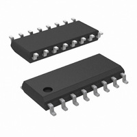
... The individual LVDS outputs can be put into TRI-STATE by use of the enable pins. For more details, please refer to the Application Information section of this datasheet. Connection Diagrams Order Number DS90CP22M-8 (SOIC) Order Number DS90CP22MT (TSSOP) © 2007 National Semiconductor Corporation Features ■ 800 Mbps low jitter, low skew operation ■ ...
Page 2
... Absolute Maximum Ratings If Military/Aerospace specified devices are required, please contact the National Semiconductor Sales Office/ Distributors for availability and specifications. Supply Voltage ( CMOS/TTL Input Voltage (EN0, EN1, SEL0, SEL1) LVDS Receiver Input Voltage (IN +, IN−) LVDS Driver Output Voltage (OUT +, OUT−) ...
Page 3
AC Electrical Characteristics Over recommended operating supply and temperature ranges unless otherwise specified (Note 4) Symbol Parameter T Input to SEL Setup Time, Figures 1, 2 SET (Note 5) T Input to SEL Hold Time, Figures 1, 2 HOLD (Note ...
Page 4
AC Timing Diagrams FIGURE 1. Input-to-Select rising edge setup and hold times and mux switch time FIGURE 2. Input-to-Select falling edge setup and hold times and mux switch time FIGURE 3. Output active to TRI-STATE and TRI-STATE to active output ...
Page 5
FIGURE 4. LVDS Output Load FIGURE 5. LVDS Output Transition Time FIGURE 6. Propagation Delay Low-to-High and High-to-Low FIGURE 7. Output Channel-to-Channel Skew in 1:2 splitter mode 5 10105306 10105309 10105307 10105308 www.national.com ...
Page 6
DS90CP22 Pin Descriptions Pin Name # of Pin IN OUT+ 2 OUT - SEL 2 GND Application Information MODES OF OPERATION The DS90CP22 provides three modes of ...
Page 7
SEL0 Note low high EN0 = EN1 = 1 for enable Typical Performance Characteristics Diff. Output Voltage (V Function Table SEL1 OUT0 OUT1 0 0 IN0 IN0 0 1 IN0 IN1 1 0 IN1 IN0 1 ...
Page 8
Peak-to-Peak Output Jitter +0.4V vs. VID CM Peak-to-Peak Output Jitter +1.2V vs. VID CM Peak-to-Peak Output Jitter +1.6V vs. VID CM 8 10105312 10105313 10105314 ...
Page 9
... Physical Dimensions inches (millimeters) unless otherwise noted 16-Lead (4.4mm Wide) Molded Thin Shrink Small Outline Package, JEDEC Order Number DS90CP22M-8 See NS Package Number M16A Order Number DS90CP22MT Order Number DS90CP22MTX (Tape and Reel) See NS Package Number MTC16 9 www.national.com ...
Page 10
... For more National Semiconductor product information and proven design tools, visit the following Web sites at: Products Amplifiers www.national.com/amplifiers Audio www.national.com/audio Clock Conditioners www.national.com/timing Data Converters www.national.com/adc Displays www.national.com/displays Ethernet www.national.com/ethernet Interface www.national.com/interface LVDS www.national.com/lvds Power Management www.national.com/power Switching Regulators www.national.com/switchers LDOs www ...