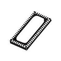
ST3DV520AQTR STMicroelectronics, ST3DV520AQTR Datasheet

ST3DV520AQTR
Specifications of ST3DV520AQTR
Available stocks
Related parts for ST3DV520AQTR
ST3DV520AQTR Summary of contents
Page 1
... MHz -3 dB typical bandwidth (or data frequency) ■ Package: QFN56 Table 1. Device summary Order code ST3DV520AQTR April 2010 Description The ST3DV520A 20- to 10-bit multiplexer /demultiplexer is a high bandwidth bidirectional switch with low R ON applications. The signal from each input is multiplexed into one of two selected outputs, while the unselected switch goes into Hi-Z status ...
Page 2
Contents Contents 1 Pin description . . . . . . . . . . . . . . . . . . . . . . . . . . . . . . . . . . . ...
Page 3
ST3DV520A 1 Pin description Figure 1. Pin connection (top through view) Table 2. Pin description Pin 11, 12, 14, 15, 19, 20 22, 23, 48, 47, 43, 42, 37, 36, 32, 31 25, 26, 46, 45, ...
Page 4
Pin description Figure 2. Input equivalent circuit Table 3. Switch function table SEL L H 4/19 Function 10-bit bus to 10-bit multiplexed bus 0 10-bit bus to 10-bit multiplexed bus 1 Doc ID 16885 Rev 2 ST3DV520A ...
Page 5
ST3DV520A 2 Maximum ratings Stressing the device above the rating listed in the “absolute maximum ratings” table may cause permanent damage to the device. These are stress ratings only and operation of the device at these or any other conditions ...
Page 6
Electrical characteristics 3 Electrical characteristics Table 6. DC electrical characteristics (V Symbol Parameter V Voltage input high (SEL) IH Voltage input low V IL (SEL) Clamp diode voltage V IK (SEL) Input high current I IH (SEL) Input low current ...
Page 7
ST3DV520A Table 7. Capacitance (T Symbol Parameter SEL pin input C IN capacitance Switch off C OFF capacitance Switch capacitance 1. Refer to Figure 5 on page 10 2. Refer to Figure 6 on page 10 3. ...
Page 8
Electrical characteristics Table 10. Switching characteristics (T Symbol Parameter t Propagation delay Line enable time, SE PZH PZL t , Line disable time, SE PHZ ...
Page 9
ST3DV520A Figure 3. Diagram for suggested V C=2uF or 4.7uF Note: 100nF Capacitors must be used as local bypass capacitors between the adjacent VDD and GND pairs (total 7) 1. Applicable for system level ESD test Figure 4. Test circuit ...
Page 10
Electrical characteristics Figure 5. Test circuit for SEL pin input capacitance (C Figure 6. Test circuit for switch off capacitance ( 0.5 Vpp 10/19 LCR meter 0.5 Vpp MHz ...
Page 11
ST3DV520A Figure 7. Test circuit for switch on capacitance (C Figure 8. Test circuit for bandwidth measurement (BW) Frequency response is measured at the output of the ON channel. For example, when and A is the input, ...
Page 12
Electrical characteristics Figure 9. Test circuit for crosstalk measurement (x Crosstalk is measured at the output of the non-adjacent ON channel. For example, when and B is the input, the output is measured at D. All unused ...
Page 13
ST3DV520A Figure 10. Test circuit for off isolation measurement (O Off isolation is measured at the output of the OFF channel. For example, when the input, the output is measured at B1. All unused analog input ports ...
Page 14
Package mechanical data 4 Package mechanical data In order to meet environmental requirements, ST offers these devices in different grades of ® ECOPACK packages, depending on their level of environmental compliance. ECOPACK specifications, grade definitions and product status are available ...
Page 15
ST3DV520A Figure 12. Mechanical data for QFN56 ( mm) - pitch 0.5 mm Symbol Figure 13. Footprint recommendation for QFN56 ( mm) - pitch ...
Page 16
Package mechanical data Figure 14. Carrier tape information for QFN56 ( mm) - pitch 0.5 mm 16/19 Doc ID 16885 Rev 2 ST3DV520A 7875978_K ...
Page 17
ST3DV520A Figure 15. Reel information for QFN56 ( mm) - pitch 0.5 mm Doc ID 16885 Rev 2 Package mechanical data 17/19 ...
Page 18
Revision history 5 Revision history Table 12. Document revision history Date 11-Dec-2009 07-Apr-2010 18/19 Revision 1 Initial release. Corrected circuit drawing errors in 2 Modified text in the Description on page Doc ID 16885 Rev 2 ST3DV520A Changes Figure 2: ...
Page 19
... ST3DV520A Information in this document is provided solely in connection with ST products. STMicroelectronics NV and its subsidiaries (“ST”) reserve the right to make changes, corrections, modifications or improvements, to this document, and the products and services described herein at any time, without notice. All ST products are sold pursuant to ST’s terms and conditions of sale. ...


