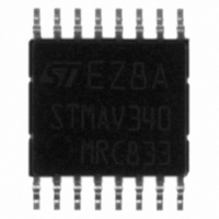
STMAV340TTR STMicroelectronics, STMAV340TTR Datasheet

STMAV340TTR
Specifications of STMAV340TTR
STMAV340TTR
Available stocks
Related parts for STMAV340TTR
STMAV340TTR Summary of contents
Page 1
... The STMAV340 is able to simplify the PCB routing on inputs and outputs as well as reduce the overall BOM costs by eliminating the need for more costly input-output controllers. Package –40°C to +85°C TSSOP16 STMAV340 TSSOP16 superior image ) of the ON Comments STMAV340TTR Rev. 1 1/21 www.st.com 21 ...
Page 2
Contents 1 Summary Description . . . . . . . . . . . . . . . . . . . . . . . . . . . . . . . . . . . . ...
Page 3
STMAV340 1 Summary Description 1.1 Functional Description The STMAV340 is a high bandwidth, analog video switch low ON-resistance and low I/O capacitance result in a very small propagation delay. When OE_N is set to LOW, the select (S) ...
Page 4
Pin Configuration 2 Pin Configuration Figure 2. Pin Configuration (Top View ) Table 1. Pin Description Symbol OE_N S 1A ,2A ,3A ,4A ...
Page 5
STMAV340 3 Application Diagrams Figure 3. STMAV340 2-to-1 Analog Video Switch Used in an LCD TV Figure 4. STMAV340 1-to-2 Analog Video Switch Used 3.1 Power Supply Sequencing Proper power-supply sequencing is advised for all CMOS devices. ...
Page 6
... These are stress ratings only and operation of the device at these or any other conditions above those indicated in the Operating sections of this specification is not implied. Exposure to Absolute Maximum Rating conditions for extended periods may affect device reliability. Refer also to the STMicroelectronics SURE Program and other relevant quality documents. Table 3. ...
Page 7
STMAV340 5 Electrical Characteristics Table 4. Recommended Operating Conditions T = -20 to +70°C A Symbol Parameter V Power Supply Voltage CC V Input Voltage IN V Output Voltage OUT t t Input Rise and Fall Time ...
Page 8
Electrical Characteristics Table 6. AC Electrical Characteristics T = -40°C to +85° Symbol Parameter Output Enable Time, Select to Bus B/C V PZH PZL Output Enable Time, OE_N to Bus A, B ...
Page 9
STMAV340 6 Test Circuit and Diagrams Note: CL includes probe and jig capacitance. All input pulses are supplied by generators having the following characteristics: PRR = 10MHz, Ω tr,tf = 2.5ns. Figure 5. AC Test Circuit ...
Page 10
Test Circuit and Diagrams Figure 6. AC Waveforms 5ns = 2. 5ns f f 90% 90% ENABLE ENABLE INPUT INPUT t t PZL PZL t t PZH PZH 10/21 10% 10% ...
Page 11
STMAV340 Figure 7. ON Resistance Test Circuit 6 Test Circuit and Diagrams 11/21 ...
Page 12
Test Circuit and Diagrams Table 8. Test Circuit V Test CC 4.75V ± 0.75V t ON 4.75V ± 0.75V 4.75V ± 0.75V t OFF 4.75V ± 0.75V Figure 8. Turn-on/Turn-off Test Circuit and Timing Diagram 12/ ...
Page 13
STMAV340 Differential gain and phase are measured at the output of the ON channel. For example, when and 1A is the input, the output is measured at 1B. SEL OE_N Figure 9. Differential Gain/Phase ...
Page 14
Test Circuit and Diagrams Frequency response is measured at the output of the ON channel. For example, when and 1A is the input, the output is measured at 1B. All unused analog I/O ports ...
Page 15
STMAV340 A 50Ω termination resistor is needed for the network analyzer. Crosstalk is measured at the output of the non-adjacent ON channel. For example, V the output is measured at 1C. All unused analog input ports are connected to GND ...
Page 16
Test Circuit and Diagrams A 50Ω termination resistor is needed for the network analyzer. Off-isolation is measured at the output of the OFF channel. For example, when V output is measured at 1B. All unsued analog input ports are ...
Page 17
STMAV340 Figure 13. I/O Pin (Input Side) ESD Protection Circuit Figure 14. I/O Pin (Output Side) ESD Protection Circuit Figure 15. S and OE_N Input ESD Protection Circuit 6 Test Circuit and Diagrams 17/21 ...
Page 18
Package Mechanical Data 7 Package Mechanical Data In order to meet environmental requirements, ST offers these devices in ECOPACK packages. These packages have a Lead-free second level interconnect . The category of second Level Interconnect is marked on the ...
Page 19
STMAV340 Figure 16. TSSOP16 Mechanical Data DIM. MIN 0.05 A2 0.85 b 0.19 c 0.09 D 4.9 E 6. PIN 1 IDENTIFICATION 1 TSSOP16 MECHANICAL DATA ...
Page 20
Revision History 8 Revision History Date Revision 09-Sep-2005 1 20/21 Description of Change First issue STMAV340 ...
Page 21
... No license is granted by implication or otherwise under any patent or patent rights of STMicroelectronics. Specifications mentioned in this publication are subject to change without notice. This publication supersedes and replaces all information previously supplied. STMicroelectronics products are not authorized for use as critical components in life support devices or systems without express written approval of STMicroelectronics ...


