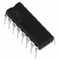
HCF4052BEY STMicroelectronics, HCF4052BEY Datasheet - Page 6

HCF4052BEY
Manufacturer Part Number
HCF4052BEY
Description
IC MUX/DEMUX DUAL 4X1 16DIP
Manufacturer
STMicroelectronics
Series
4000Br
Type
Analog Multiplexerr
Datasheet
1.HCF4052M013TR.pdf
(11 pages)
Specifications of HCF4052BEY
Function
Multiplexer/Demultiplexer
Circuit
2 x 4:1
On-state Resistance
280 Ohm
Voltage Supply Source
Dual Supply
Voltage - Supply, Single/dual (±)
±3 V ~ 20 V
Current - Supply
.08µA
Operating Temperature
-55°C ~ 125°C
Mounting Type
Through Hole
Package / Case
16-DIP (0.300", 7.62mm)
Number Of Channels
2 Channel
On Resistance (max)
1050 Ohms
Propagation Delay Time
60 ns
On Time (max)
720 ns
Off Time (max)
450 ns
Supply Voltage (max)
20 V
Supply Voltage (min)
3 V
Maximum Power Dissipation
500 mW
Maximum Operating Temperature
+ 125 C
Minimum Operating Temperature
- 55 C
Mounting Style
Through Hole
Number Of Switches
2
Package
16PDIP
Maximum On Resistance
1050@5V Ohm
Maximum Propagation Delay Bus To Bus
20@15V|30@10V|60@5V ns
Multiplexer Architecture
4:1
Maximum Turn-off Time
450@5V ns
Maximum Turn-on Time
720@5V ns
Power Supply Type
Single
Lead Free Status / RoHS Status
Contains lead / RoHS non-compliant
Other names
497-1362-5
Available stocks
Company
Part Number
Manufacturer
Quantity
Price
Company:
Part Number:
HCF4052BEY
Manufacturer:
IBM
Quantity:
2 836
HCF4052B
TYPICAL BIAS VOLTAGES
The ADDRESS (digtal-control inputs) and INHIBIT logic levels are : "0"=V
from V
TYPICAL APPLICATIONS (TYPICAL TIME-DIVISION APPLICATION)
SPECIAL CONSIDERATIONS
Control of analog signals up to 20V peak to peak
can be achieved by digital signal amplitudes of 4.5
to 20V (if V
can be controlled; for V
above 13V, a V
required. For example, if V
V
can be controlled by digital inputs of 0 to 4.5V. In
certain applications, the external load resistor
6/11
EE
= -13.5, analog signals from -13.5V to 4.5V
EE
to V
DD
DD
- V
SS
DD
= 3V, a V
- V
DD
SS
- V
DD
DD
of at least 4.5V is
EE
= +5, V
- V
level differences
EE
of up to 13V
SS
= 0, and
current may include both V
components. To avoid drawing V
switch current flows into the transmission gate
inputs, the voltage drop across the bidirectional
switch must not exceed 0,8V (calculated from R
values shown in DC SPECIFICATIONS). No V
current will flow through R
flows into leads 3 and 13.
SS
and "1"=V
DD
. The analog signal (through the TG) may swing
L
if the switch current
DD
DD
and signal-line
current when
ON
DD


