HCF4051BEY STMicroelectronics, HCF4051BEY Datasheet
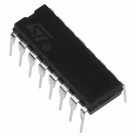
IC MUX/DEMUX 8X1 16DIP

HCF4051BEY

Manufacturer Part Number
HCF4051BEY
Description
IC MUX/DEMUX 8X1 16DIP
Manufacturer
STMicroelectronics
Series
4000Br
Type
Analog Multiplexerr
Datasheets

Specifications of HCF4051BEY

Function
Multiplexer/Demultiplexer
Circuit
1 x 8:1
On-state Resistance
280 Ohm
Voltage Supply Source
Dual Supply
Voltage - Supply, Single/dual (±)
±3 V ~ 20 V
Current - Supply
.08µA
Operating Temperature
-55°C ~ 125°C
Mounting Type
Through Hole
Package / Case
16-DIP (0.300", 7.62mm)
Number Of Channels
1 Channel
On Resistance (max)
1050 Ohms
Propagation Delay Time
60 ns
On Time (max)
720 ns
Off Time (max)
450 ns
Supply Voltage (max)
20 V
Supply Voltage (min)
3 V
Maximum Power Dissipation
200 mW
Maximum Operating Temperature
+ 125 C
Minimum Operating Temperature
- 55 C
Mounting Style
Through Hole
Number Of Switches
Single
Capacitance, Input
5 pF (Typ.) @ 25 °C
Circuit Type
Monolithic Integrated
Current, Input
± 10 mA
Current, Input, Leakage
± 1 μA (Max.)
Current, Supply
3000 μA
Function Type
8-Channels
Logic Function
Multiplexer/Demultiplexer
Logic Type
MOS
Number Of Circuits
Single
Package Type
DIP-16
Power Dissipation
500 mW @ 65 °C
Temperature, Operating, Maximum
125 °C
Temperature, Operating, Minimum
-55 °C
Temperature, Operating, Range
-55 to +125 °C
Time, Delay, Propagation
30 ns (Typ.)
Voltage, Supply
3 to 20 V
Low In.onin. Resistance
125W (Typ.) over 15V p.p signal-input range for VDD - VEE == 15V
High In.offin. Resistance
channel leakage +⁄- 100pA (Typ.) at VDD - VEE == 18V
High Degree Of Linearity
0.5%
Package
16PDIP
Maximum On Resistance
1050@5V Ohm
Maximum Propagation Delay Bus To Bus
20@15V|30@10V|60@5V ns
Multiplexer Architecture
8:1
Maximum Turn-off Time
450@5V ns
Maximum Turn-on Time
720@5V ns
Power Supply Type
Single
Lead Free Status / RoHS Status
Lead free / RoHS Compliant
Other names
497-1361-5

Available stocks

Company
Part Number
Manufacturer
Quantity
Price
Part Number:
HCF4051BEY
Manufacturer:
ST
0
Company:
Part Number:
HCF4051BEY
Quantity:
3 000
PIN CONNECTION
LOW "ON" RESISTANCE : 125
OVER 15V p.p SIGNAL-INPUT RANGE FOR
V
HIGH "OFF" RESISTANCE : CHANNEL
LEAKAGE
BINARY ADDRESS DECODING ON CHIP
HIGH DEGREE OF LINEARITY : < 0.5%
DISTORTION TYP. at f
V
VERY LOW QUIESCENT POWER
DISSIPATION UNDER ALL DIGITAL
CONTROL INPUT AND SUPPLY
CONDITIONS : 0.2 W (Typ.)
at V
MATCHED SWITCH CHARACTERISTICS :
R
WIDE RANGE OF DIGITAL AND ANALOG
SIGNAL LEVELS : DIGITAL 3 to 20,
ANALOG TO 20V p.p.
QUIESCENT CURRENT SPECIFIED UP TO
20V
5V, 10V AND 15V PARAMETRIC RATINGS
INPUT LEAKAGE CURRENT
I
100% TESTED FOR QUIESCENT CURRENT
MEETS ALL REQUIREMENTS OF JEDEC
JESD13B " STANDARD SPECIFICATIONS
FOR DESCRIPTION OF B SERIES CMOS
DEVICES"
I
DD
DD
ON
= 100nA (MAX) AT V
DD
- V
- V
= 5 (Typ.) FOR V
- V
EE
SS
SS
= 15V
> 10V, RL = 10K
= V
100pA (Typ.) at V
DD
- V
EE
DD
IS
DD
= 1KHz, V
=10V
= 18V T
- V
ANALOG MULTIPLEXER/DEMULTIPLEXER
EE
DD
= 15V
A
(Typ.)
- V
= 25°C
IS
EE
= 5 V
= 18V
pp
,
ORDER CODES
DESCRIPTION
The HCF4051B is a monolithic integrated circuit
fabricated
technology available in DIP and SOP packages.
The HCF4051B analog multiplexer/demultiplexer
is a digitally controlled analog switch having low
ON impedance and very low OFF leakage current.
This multiplexer circuit dissipate extremely low
quiescent power over the full V
V
logic state of the control signals.
When a logic "1" is present at the inhibit input
terminal all channel are off. This device is a single
8-channel multiplexer having three binary control
inputs, A, B, and C, and an inhibit input. The three
binary signals select 1 of 8 channels to be turned
on, and connect one of the 8 inputs to the output.
PACKAGE
EE
SOP
DIP
supply voltage range, independent of the
in
DIP
HCF4051BM1
HCF4051BEY
SINGLE 8-CHANNEL
Metal
TUBE
Oxide
HCF4051B
DD
HCF4051M013TR
SOP
- V
Semiconductor
SS
T & R
and V
DD
1/10
-

Related parts for HCF4051BEY

HCF4051BEY Summary of contents

Page 1

... A, B, and C, and an inhibit input. The three binary signals select channels to be turned on, and connect one of the 8 inputs to the output. HCF4051B SINGLE 8-CHANNEL DIP SOP TUBE HCF4051BEY HCF4051BM1 HCF4051M013TR in Metal Oxide Semiconductor - V DD supply voltage range, independent of the T & ...

Page 2

ABSOLUTE MAXIMUM RATINGS Symbol V Supply Voltage Input Voltage Input Current I P Power Dissipation per Package D Power Dissipation per Output Transistor T Operating Temperature op T Storage Temperature stg Absolute Maximum Ratings ...

Page 3

HCF4051B DC SPECIFICATIONS Symbol Parameter V (V) I Quiescent Device L Current (all switches ON or all switches OFF) SWITCH R Resistance ON 0 < Resistance ON RON 0 < V (between any switches) ...

Page 4

DYNAMIC ELECTRICAL CHARACTERISTICS (T fall time = Parameter Propagation Delay Time (signal input to output) Frequency Response Channel "ON" (sine = V wave input log ...

Page 5

HCF4051B DIM. MIN. a1 0. 8/10 Plastic DIP-16 (0.25) MECHANICAL DATA mm. TYP MAX. 1.65 0.5 0.25 20 8.5 2.54 17.78 7.1 5.1 3.3 1.27 inch MIN. TYP. ...

Related keywords