TDA8541 NXP Semiconductors, TDA8541 Datasheet
TDA8541
Specifications of TDA8541
Available stocks


Related parts for TDA8541


TDA8541 Summary of contents
Page 1
... DATA SHEET TDA8541 1 W BTL audio amplifier Product specification Supersedes data of 1997 Feb 19 INTEGRATED CIRCUITS 1998 Apr 01 ...
Page 2
... The TDA8541( one channel audio power amplifier for an output power with an 8 Ω load supply. The circuit contains a BTL amplifier with a complementary PNP-NPN output stage and standby/mute logic. The TDA8541T comes pin SO package and the TDA8541 pin DIP package. APPLICATIONS • Portable consumer products • ...
Page 3
... MODE STANDBY/MUTE LOGIC Fig.1 Block diagram. FUNCTIONAL DESCRIPTION The TDA8541( BTL audio power amplifier capable of delivering 1 W output power Ω load at THD = 10% using power supply. Using the MODE pin the device can be switched to standby and mute condition. The device is protected by an internal thermal shutdown protection mechanism ...
Page 4
... In accordance with “SNW-FQ-611-E”. The number of the quality specification can be found in the “Quality Reference Handbook”. The handbook can be ordered using the code 9397 750 00192. THERMAL CHARACTERISTICS SYMBOL R thermal resistance from junction to ambient th j-a TDA8541T (SO8) TDA8541 (DIP8) DC CHARACTERISTICS = 25 ° Ω ...
Page 5
... CONDITIONS MIN. THD = 10% 1 THD = 0.5% 0.6 − 0 note 1 6 − − note 2 note 3 50 note 4 40 − note 5 5 Product specification TDA8541 TYP. MAX. UNIT − 1.2 W − 0.9 W 0.15 0.3 % − − 100 kΩ − μV 100 − − ...
Page 6
... The frequency characteristic can be adapted by connecting a small capacitor across the feedback resistor. To improve the immunity of HF radiation in radio circuit = applications, a small capacitor can be connected in parallel with the feedback resistor (56 kΩ); this creates a low-pass filter function ms 6 Product specification TDA8541 Ω dB, audio band-pass 7.5 V, ...
Page 7
... V q 1998 Apr 01 56 kΩ − TDA8541 SVR 2 MODE GND Fig.3 BTL application. MGD876 handbook, halfpage ( 100 μF 100 nF OUT − OUT + 8 MBH881 10 THD (%) (1) 1 −1 10 −2 10 −2 − kHz dB Ω. ( Ω. ( Fig.5 THD as a function of P Product specification TDA8541 MGD877 ( ( ...
Page 8
... V CC (1) G (2) G (3) G MGD880 handbook, halfpage ( (V) (1) R (2) R Fig Product specification −20 −40 (1) (2) −60 (3) − Ω Ω 100 dB. v Fig.7 SVRR as a function of frequency (W) 1.5 (1) ( Ω Ω. L Worst case power dissipation as a function TDA8541 MGD879 (Hz) MGD881 (V) ...
Page 9
... Sine wave of 1 kHz Ω. ( Ω. ( Fig. function handbook, halfpage V ms (V) 12 standby Fig. function 1998 Apr 01 MGD882 handbook, halfpage 1 MGL070 mute operating ( (V) 1 −1 10 −2 10 (1) (2) (3) −3 10 −4 10 −5 10 −6 10 − Band-pass = kHz Fig. function Product specification TDA8541 MGD883 ( ...
Page 10
... TDA8541 SVR 2 MODE GND Fig.13 SE application. MGD884 handbook, halfpage (W) P (1) V ( 100 μF 100 nF C3 OUT − 5 470 μ OUT + 8 MBH882 10 THD (%) 1 (1) −1 10 (2) (3) − 0 dB Ω Ω Ω Fig.15 THD as a function of frequency. Product specification TDA8541 MGD885 (Hz) ...
Page 11
... THD = 10%, R (2) THD = 10%, R (3) THD = 10%, R MGD888 handbook, halfpage ( (V) (1) V (2) V (3) V Fig.19 Power dissipation as a function Product specification 2 (1) ( Ω Ω Ω. L Fig. function 1.2 P (1) (W) (2) 0.8 (3) 0 0.4 0 Ω Ω Ω TDA8541 MGD887 ( ( MGD889 1 ...
Page 12
... NXP Semiconductors 1 W BTL audio amplifier handbook, full pagewidth 1998 Apr 01 a. Top view. 6.8 kΩ MS 6.8 kΩ 1 TDA8541 1 μ kΩ μF 100 μF b. Component side. Fig.20 Printed-circuit board layout (BTL and SE). 12 Product specification 8 OUT + OUT − kΩ 100 MBH920 TDA8541 ...
Page 13
... REFERENCES JEDEC JEITA MS-012 θ detail 6.2 1.0 0.7 1.05 0.25 0.25 5.8 0.4 0.6 0.244 0.039 0.028 0.041 0.01 0.01 0.228 0.016 0.024 EUROPEAN PROJECTION Product specification TDA8541 SOT96 (1) θ 0.7 0 0.028 0.004 0.012 ISSUE DATE 99-12-27 03-02-18 ...
Page 14
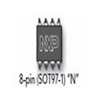
... REFERENCES JEDEC JEITA MO-001 SC-504 ( 6.48 3.60 8.25 2.54 7.62 6.20 3.05 7.80 0.26 0.14 0.32 0.1 0.3 0.24 0.12 0.31 EUROPEAN PROJECTION Product specification TDA8541 SOT97-1 ( max. 10.0 0.254 1.15 8.3 0.39 0.01 0.045 0.33 ISSUE DATE 99-12-27 03-02-13 ...
Page 15
... Use only a low voltage soldering iron (less than 24 V) applied to the flat part of the lead. Contact time must be limited to 10 seconds 300 °C. When using a dedicated tool, all other leads can be soldered in one operation within seconds between 270 and 320 °C. 15 Product specification TDA8541 ...
Page 16
... NXP Semiconductors products in order to avoid a default of the applications and the products or of the application or use by customer’s third party customer(s). NXP does not accept any liability in this respect. 16 Product specification TDA8541 DEFINITION ...
Page 17
... NXP Semiconductors for any liability, damages or failed product claims resulting from customer design and use of the product for automotive applications beyond NXP Semiconductors’ standard warranty and NXP Semiconductors’ product specifications. 17 Product specification TDA8541 ...
Page 18
... Interface, Security and Digital Processing expertise Customer notification This data sheet was changed to reflect the new company name NXP Semiconductors, including new legal definitions and disclaimers. No changes were made to the technical content, except for package outline drawings which were updated to the latest version. ...