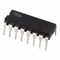
HEF4052BP,652 NXP Semiconductors, HEF4052BP,652 Datasheet - Page 2

HEF4052BP,652
Manufacturer Part Number
HEF4052BP,652
Description
IC MUX/DEMUX DUAL 4X1 16DIP
Manufacturer
NXP Semiconductors
Series
4000Br
Type
Analog Multiplexerr
Specifications of HEF4052BP,652
Package / Case
16-DIP (0.300", 7.62mm)
Function
Multiplexer/Demultiplexer
Circuit
2 x 4:1
On-state Resistance
175 Ohm
Voltage Supply Source
Single Supply
Voltage - Supply, Single/dual (±)
3 V ~ 15 V, -18 V ~ 0.5 V
Operating Temperature
-40°C ~ 85°C
Mounting Type
Through Hole
Number Of Channels
2 Channel
On Resistance (max)
2500 Ohm @ 5 V
On Time (max)
260 ns @ 5 V
Off Time (max)
205 ns @ 5 V
Supply Voltage (max)
15.5 V
Supply Voltage (min)
4.5 V
Mounting Style
Through Hole
Number Of Switches
Dual
Package
16PDIP
Maximum On Resistance
2500@5V Ohm
Maximum Propagation Delay Bus To Bus
305@5V|150@10V|100@15V ns
Maximum Low Level Output Current
10 mA
Multiplexer Architecture
4:1
Maximum Turn-off Time
205@5V ns
Maximum Turn-on Time
260@5V ns
Power Supply Type
Single
Lead Free Status / RoHS Status
Lead free / RoHS Compliant
Lead Free Status / RoHS Status
Lead free / RoHS Compliant, Lead free / RoHS Compliant
Other names
568-3109-5
933282430652
HEF4052BPN
933282430652
HEF4052BPN
Philips Semiconductors
DESCRIPTION
The HEF4052B is a dual 4-channel
analogue multiplexer/demultiplexer
with common channel select logic.
Each multiplexer/demultiplexer has
four independent inputs/outputs
(Y
(Z). The common channel select logic
includes two address inputs (A
A
(E).
January 1995
1
0
) and an active LOW enable input
Dual 4-channel analogue multiplexer/demultiplexer
to Y
3
) and a common input/output
Fig.1 Functional diagram.
0
and
Both multiplexers/demultiplexers
contain four bidirectional analogue
switches, each with one side
connected to an independent
input/output (Y
side connected to a common
input/output (Z).
With E LOW, one of the four switches
is selected (low impedance ON-state)
by A
switches are in the high impedance
OFF-state, independent of A
0
and A
1
. With E HIGH, all
0
to Y
2
3
) and the other
0
and A
1
.
PINNING
FAMILY DATA,
I
See Family Specifications
DD
Y
Y
A
E
Z
HEF4052BP(N): 16-lead DIL; plastic
HEF4052BD(F): 16-lead DIL; ceramic
HEF4052BT(D): 16-lead SO; plastic
( ): Package Designator North America
A
0A
0B
0
, A
V
connections for the digital control
inputs (A
V
inputs/outputs (Y
swing between V
and V
V
For operation as a digital
multiplexer/demultiplexer, V
connected to V
, Z
LIMITS category MSI
DD
SS
DD
to Y
to Y
B
1
range is 3 to 15 V. The analogue
and V
Fig.2 Pinning diagram.
3A
3B
EE
V
EE
as a negative limit.
0
, A
SS
may not exceed 15 V.
independent inputs/outputs
independent inputs/outputs
address inputs
enable input (active LOW)
common inputs/outputs
1
are the supply voltage
and E). The V
Product specification
SS
(cerdip)
(SOT38-1)
(SOT74)
(SOT109-1)
DD
0
HEF4052B
(typically ground).
to Y
as a positive limit
3
, and Z) can
EE
DD
MSI
is
to


