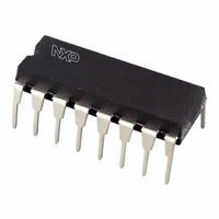
HEF4052BP,652 NXP Semiconductors, HEF4052BP,652 Datasheet - Page 12

HEF4052BP,652
Manufacturer Part Number
HEF4052BP,652
Description
IC MUX/DEMUX DUAL 4X1 16DIP
Manufacturer
NXP Semiconductors
Series
4000Br
Type
Analog Multiplexerr
Specifications of HEF4052BP,652
Package / Case
16-DIP (0.300", 7.62mm)
Function
Multiplexer/Demultiplexer
Circuit
2 x 4:1
On-state Resistance
175 Ohm
Voltage Supply Source
Single Supply
Voltage - Supply, Single/dual (±)
3 V ~ 15 V, -18 V ~ 0.5 V
Operating Temperature
-40°C ~ 85°C
Mounting Type
Through Hole
Number Of Channels
2 Channel
On Resistance (max)
2500 Ohm @ 5 V
On Time (max)
260 ns @ 5 V
Off Time (max)
205 ns @ 5 V
Supply Voltage (max)
15.5 V
Supply Voltage (min)
4.5 V
Mounting Style
Through Hole
Number Of Switches
Dual
Package
16PDIP
Maximum On Resistance
2500@5V Ohm
Maximum Propagation Delay Bus To Bus
305@5V|150@10V|100@15V ns
Maximum Low Level Output Current
10 mA
Multiplexer Architecture
4:1
Maximum Turn-off Time
205@5V ns
Maximum Turn-on Time
260@5V ns
Power Supply Type
Single
Lead Free Status / RoHS Status
Lead free / RoHS Compliant
Lead Free Status / RoHS Status
Lead free / RoHS Compliant, Lead free / RoHS Compliant
Other names
568-3109-5
933282430652
HEF4052BPN
933282430652
HEF4052BPN
NXP Semiconductors
Table 10.
[1]
HEF4052B_7
Product data sheet
Input
nYn, nZ
V
Fig 16. Test circuit for measuring switching times
DD
For nYn to nZ propagation delays use V
or V
EE
Test data is given in
Definitions:
DUT = Device Under Test.
R
C
R
T
L
L
Test data
Sn and E
V
= Load capacitance including test jig and probe.
= Load resistance.
= Termination resistance should be equal to output impedance Z
DD
or V
SS
t
≤ 20 ns
r
, t
Table
f
10.
GENERATOR
negative
V
0.5V
positive
M
PULSE
pulse
pulse
EE
DD
. For Sn to nYn or nZ propagation delays use V
All information provided in this document is subject to legal disclaimers.
0 V
0 V
V
V
I
I
Load
C
50 pF
90 %
10 %
V I
L
Rev. 07 — 26 March 2010
t
t
f
r
R T
V
V
V
M
M
90 %
DD
10 %
DUT
R
10 kΩ
L
V
I
t
t
W
W
V O
Dual 4-channel analog multiplexer/demultiplexer
S1 position
t
V
PHL
DD
o
C L
of the pulse generator.
V
V
R L
[1]
or V
M
M
t
t
r
f
EE
S1
V
001aaj903
t
V
DD
PLH
EE
open
DD
V
V
.
SS
EE
t
V
PZH
EE
, t
PHZ
HEF4052B
© NXP B.V. 2010. All rights reserved.
t
V
PZL
DD
, t
PLZ
other
V
12 of 22
EE


