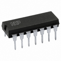
HEF4066BP,652 NXP Semiconductors, HEF4066BP,652 Datasheet - Page 5

HEF4066BP,652
Manufacturer Part Number
HEF4066BP,652
Description
IC SWITCH QUAD 1X1 14DIP
Manufacturer
NXP Semiconductors
Series
4000Br
Type
Analog Switchr
Specifications of HEF4066BP,652
Package / Case
14-DIP (0.300", 7.62mm)
Function
Switch
Circuit
4 x 1:1
On-state Resistance
175 Ohm
Voltage Supply Source
Dual Supply
Voltage - Supply, Single/dual (±)
±3 V ~ 15 V
Current - Supply
4µA
Operating Temperature
-40°C ~ 85°C
Mounting Type
Through Hole
Switch Configuration
SPST
On Resistance (max)
2500 Ohm @ 5 V
On Time (max)
90 ns @ 5 V
Off Time (max)
160 ns @ 5 V
Supply Voltage (max)
15.5 V
Supply Voltage (min)
4.5 V
Maximum Power Dissipation
100 mW
Maximum Operating Temperature
+ 85 C
Mounting Style
Through Hole
Minimum Operating Temperature
- 40 C
Propagation Delay Time
5 ns
Package
14PDIP
Maximum On Resistance
2500@5V Ohm
Maximum Propagation Delay Bus To Bus
20@5V|10@10V|10@15V ns
Maximum Low Level Output Current
10 mA
Maximum Turn-off Time
160@5V ns
Maximum Turn-on Time
90@5V ns
Switch Architecture
SPST
Power Supply Type
Single
Lead Free Status / RoHS Status
Lead free / RoHS Compliant
Lead Free Status / RoHS Status
Lead free / RoHS Compliant, Lead free / RoHS Compliant
Other names
568-1694-5
933296650652
HEF4066BPN
933296650652
HEF4066BPN
NXP Semiconductors
Table 7.
T
HEF4066B_6
Product data sheet
Symbol
R
R
ΔR
amb
Fig 5.
ON(peak)
ON(rail)
ON
= 25
°
R
Test circuit for measuring R
C; I
V
Parameter
ON resistance (peak)
ON resistance (rail)
ON resistance mismatch
between channels
ON
ON resistance
IH
SW
= V
10.2.1 ON resistance waveform and test circuit
10.2 ON resistance
SW
= 200
V I
/ I
SW
μ
.
nE
nY
A; V
V
V
SS
SW
DD
V
SS
= 0 V.
nZ
ON
Conditions
V
Figure 6
V
V
V
001aak670
I
I
I
I
All information provided in this document is subject to legal disclaimers.
= 0 V to V
= 0 V; see
= V
= 0 V to V
DD
I SW
; see
Rev. 06 — 25 March 2010
DD
DD
Figure 5
Figure 5
; see
; see
Figure 5
Figure 5
and
and
Fig 6.
Figure 6
R
Figure 6
(Ω)
(1) V
(2) V
(3) V
ON
400
300
200
100
and
Quad single-pole single-throw analog switch
0
0
I
Typical R
SW
DD
DD
DD
(2)
(3)
= 200 μA.
= 5 V
= 10 V
= 15 V
V
10 V
15 V
10 V
15 V
10 V
15 V
10 V
15 V
5 V
5 V
5 V
5 V
DD
(1)
ON
as a function of input voltage
5
Typ
350
80
60
115
50
40
120
65
50
25
10
5
10
HEF4066B
© NXP B.V. 2010. All rights reserved.
V
Max
2500
245
175
340
160
115
365
200
155
-
-
-
I
001aak671
(V)
15
Unit
Ω
Ω
Ω
Ω
Ω
Ω
Ω
Ω
Ω
Ω
Ω
Ω
5 of 16


