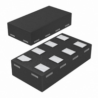
74LVC2G66GT,115 NXP Semiconductors, 74LVC2G66GT,115 Datasheet - Page 15

74LVC2G66GT,115
Manufacturer Part Number
74LVC2G66GT,115
Description
IC SWITCH DUAL SPST 8XSON
Manufacturer
NXP Semiconductors
Series
74LVCr
Type
Analog Switchr
Datasheet
1.74LVC2G66GM125.pdf
(26 pages)
Specifications of 74LVC2G66GT,115
Package / Case
8-XFDFN
Function
Switch
Circuit
2 x SPST - NO
On-state Resistance
6 Ohm
Voltage Supply Source
Single Supply
Voltage - Supply, Single/dual (±)
1.65 V ~ 5.5 V
Current - Supply
0.1µA
Operating Temperature
-40°C ~ 125°C
Mounting Type
Surface Mount
Switch Configuration
SPST
On Resistance (max)
34 Ohm (Typ) @ 1.95 V
On Time (max)
4.6 ns (Typ) @ 1.95 V
Off Time (max)
3.8 ns (Typ) @ 1.95 V
Supply Voltage (max)
5.5 V
Supply Voltage (min)
1.65 V
Maximum Power Dissipation
250 mW
Maximum Operating Temperature
+ 125 C
Mounting Style
SMD/SMT
Minimum Operating Temperature
- 40 C
Switch Current (typ)
0.0001 mA @ 5.5 V
Package
8XSON
Maximum On Resistance
195@1.95V Ohm
Maximum Propagation Delay Bus To Bus
0.8(Typ)@1.95V|0.4(Typ)@2.7V|0.3(Typ)@3.6V|0.2(Typ)@5.5V ns
Maximum Low Level Output Current
50 mA
Maximum Turn-off Time
3.8(Typ)@1.95V ns
Maximum Turn-on Time
4.6(Typ)@1.95V ns
Switch Architecture
SPST
Power Supply Type
Single
Lead Free Status / RoHS Status
Lead free / RoHS Compliant
Lead Free Status / RoHS Status
Lead free / RoHS Compliant, Lead free / RoHS Compliant
Other names
568-4652-2
74LVC2G66GT-G
74LVC2G66GT-G
935280087115
74LVC2G66GT-G
74LVC2G66GT-G
935280087115
NXP Semiconductors
74LVC2G66
Product data sheet
Fig 20. Test circuit for measuring total harmonic distortion
Fig 21. Test circuit for measuring the frequency response when switch is in ON-state
Fig 22. Test circuit for measuring isolation (OFF-state)
Test conditions:
V
V
V
V
Adjust f
Adjust f
CC
CC
CC
CC
= 1.65 V: V
= 2.3 V: V
= 3 V: V
= 4.5 V: V
11.3 Test circuits
i
i
voltage to obtain 0 dBm level at output. Increase f
voltage to obtain 0 dBm level at input.
i
= 2.5 V (p-p).
i
i
= 2 V (p-p).
= 4 V (p-p).
i
= 1.4 V (p-p).
f i
f i
V
IH
V
IH
0.1 μF
0.1 μF
f i
50 Ω
All information provided in this document is subject to legal disclaimers.
50 Ω
0.5V
nY/nZ
600 Ω
nY/nZ
CC
nE
R L
nE
Rev. 5 — 16 June 2010
V
IL
nY/nZ
nE
V
CC
V
CC
i
V
frequency until dB meter reads −3 dB.
nZ/nY
CC
nZ/nY
0.5V
0.5V
nZ/nY
CC
R L
CC
R L
C L
C L
10 μF
C L
0.5V
001aag492
dB
dB
D
CC
001aag491
R L
001aag493
V
O
V
V
O
O
74LVC2G66
© NXP B.V. 2010. All rights reserved.
Bilateral switch
15 of 26


