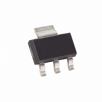
DS2405Z/T&R Maxim Integrated Products, DS2405Z/T&R Datasheet

DS2405Z/T&R
Specifications of DS2405Z/T&R
Related parts for DS2405Z/T&R
DS2405Z/T&R Summary of contents
Page 1
FEATURES Open-drain PIO pin is controlled by matching 64-bit, laser-engraved registration number associated with each device Logic level of open drain output can be ® determined over 1-Wire control PIO pin sink capability is greater than 4mA at 0.4V ...
Page 2
ORDERING INFORMATION DS2405 TO-92 package DS2405Z 4-pin SOT-223 package DS2405P 6-pin TSOC package DS2405/T&R Tape & Reel version of DS2405 DS2405Z/T&R Tape & Reel version of DS2405Z DS2405P/T&R Tape & Reel version of DS2405P DESCRIPTION The DS2405 Addressable Switch is ...
Page 3
Hardware Configuration The 1-Wire bus has only a single line by definition important that each device on the bus be able to drive it at the appropriate time. To facilitate this, each device attached to the 1-Wire bus ...
Page 4
BUS MASTER CIRCUIT Figure 3 TRANSACTION SEQUENCE The sequence for accessing the DS2405 via the 1-Wire port is as follows: Initialization ROM Function Command Read Data INITIALIZATION All transactions on the 1-Wire bus begin with an initialization sequence. The initialization ...
Page 5
ROM FUNCTION COMMANDS Once the bus master has detected a presence, it can issue one of five ROM function commands. All ROM function commands are 8 bits long. A list of these commands follows (refer to flowchart in Figure 4). ...
Page 6
The master reads 1 bit from the 1-Wire bus. Each device will respond by placing the value of the first bit of its respective ROM data onto the 1-Wire bus. Devices 1 and 4 will place a 0 onto ...
Page 7
The master must learn the other devices’ ROM data. Therefore it starts another ROM Search sequence by repeating steps 13 to 15. 19. At the highest bit position where the master wrote the previous pass (step ...
Page 8
CONTROL must be a logical 0 and the PIO pin is being held low by some other device or perhaps a fault condition such as a PIO shorted to ground. A second ...
Page 9
ROM FUNCTIONS FLOW CHART Figure ...
Page 10
ROM FUNCTIONS FLOW CHART Figure 4 (cont ...
Page 11
Skip ROM [CCh] The complete 1-Wire protocol for all Dallas Semiconductor iButtons contains a Skip ROM command. Since the DS2405 contains only the 64-bit ROM with no additional data fields, the Skip ROM is not applicable and will cause no ...
Page 12
READ/WRITE TIME SLOTS The definitions of write and read time slots are illustrated in Figure 6. All time slots are initiated by the master driving the data line low. The falling edge of the data line synchronizes the DS2405 to ...
Page 13
READ/WRITE TIMING DIAGRAM Figure 6 (cont.) Read-Data Time Slot RESISTOR MASTER DS2405 CRC GENERATION To validate the data transmitted from the DS2405, the bus master may generate a CRC value from the data received. This generated value ...
Page 14
ABSOLUTE MAXIMUM RATINGS* Voltage on any Pin Relative to Ground Operating Temperature Range Storage Temperature Range Solder Temperature ∗ This is a stress rating only and functional operation of the device at these or any other conditions above those indicated ...
Page 15
NOTES: 1. All voltages are referenced to ground external pullup voltage. PUP 3. Input load is to ground additional reset or communication sequence cannot begin until the reset high time has expired. 5. Read data ...


