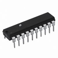
TP3420AN308 National Semiconductor, TP3420AN308 Datasheet - Page 11

TP3420AN308
Manufacturer Part Number
TP3420AN308
Description
IC INTERFACE DEVICE ISDN 20-DIP
Manufacturer
National Semiconductor
Datasheet
1.TP3420AV308-TRNOPB.pdf
(32 pages)
Specifications of TP3420AN308
Applications
*
Interface
*
Voltage - Supply
*
Package / Case
20-DIP (0.300", 7.62mm)
Mounting Type
Through Hole
Lead Free Status / RoHS Status
Contains lead / RoHS non-compliant
Other names
*TP3420AN308
Available stocks
Company
Part Number
Manufacturer
Quantity
Price
Company:
Part Number:
TP3420AN308
Manufacturer:
NS
Quantity:
6 231
Part Number:
TP3420AN308
Manufacturer:
N/A
Quantity:
20 000
D Channel Access
D Channel Request, Class 1 Message
D Channel Request, Class 2 Message
D Channel Access Control
Enable D-Channel Access Mechanism, TE Mode (Note 8)
Disable D-Channel Access Mechanism, TE Mode (Note 8)
Force Echo Bit to 0
Force Echo Bit to Inverted Received D Bit
Reset EBITI and EBIT0 to Normal Condition (Note 6)
D Channel Clock Enable
End of Message Interrupt
EOM Interrupt Enabled (Note 6)
EOM Interrupt Disabled
Multiframe Circuit and Interrupt
Enable SC1/Q Messaging and MFR1 Interrupt
Disable SC1/Q Message and Interrupt (Note 6)
Enable 5 ms Interrupt (Every Multiframe)
Disable 5 ms Interrupt (Note 6)
Enable 30 ms Interrupt (6 Multiframes)
Disable 30 ms Interrupt (Note 6)
Enable SC2 Messaging and MFR2 Interrupt
Disable SC2 Messaging and Interrupt (Note 6)
Multiframe Receive Message Validation
Enable 3x and 1x Validation of Received Data
Disable 3x and 1x Validation of Received Data (Note 6)
Multiframe Transmit Registers
Write to Multiframe Transmit Register
(SC1/Q Low Priority Messages)
Write to Multiframe Transmit Register
(SC1/Q High Priority Messages)
Write to Multiframe Transmit Register
(SC2 Messages)
B1 Channel Enable/Disable
B1 Channel Enabled
B1 Channel Disabled (Note 6)
B2 Channel Enable/Disable
B2 Channel Enabled
B2 Channel Disabled (Note 6)
Loopback Test Modes
Loopback B1 Towards Line Interface
Loopback B2 Towards Line Interface
Loopback 2B+D Towards Digital Interface
Loopback B1 Towards Digital Interface
Loopback B2 Towards Digital Interface
Clear All Loopbacks (Note 6)
Control Device State Reading
Enable the Device State Output on the NOCST
Functional Description
Function
TABLE 4. Control Register Functions (Continued)
(Continued)
DREQ1
DREQ2
DACCE
DACCD
EBIT0
EBITI
EBITNRM
DCKE
EIE
EID
MIE1
MID1
MFC1E
MFC1D
MFC6E
MFC6D
MIE2
MID2
ENV
DISV
MFT1L
MFT1H
MFT2
B1E
B1D
B2E
B2D
LBL1
LBL2
LBS
LBB1
LBB2
CAL
ENST
Mnemonic
11
7
0
0
1
1
1
1
1
1
0
0
0
0
0
0
0
0
0
0
0
0
0
0
0
0
0
0
0
0
0
0
0
0
0
1
6
0
0
0
0
0
0
0
1
0
0
0
0
0
0
0
0
0
0
0
0
0
1
1
0
0
0
0
0
0
0
0
0
0
0
5
0
0
0
0
0
0
0
1
0
0
0
0
1
1
1
1
1
1
1
1
1
0
0
0
0
0
0
0
0
0
0
0
0
0
Bit Number
4
0
0
1
1
1
1
1
1
1
1
1
1
0
0
0
0
0
0
0
0
1
0
1
1
1
1
1
1
1
1
1
1
1
1
M1
M1
M1
3
1
1
0
0
0
0
1
0
0
0
0
0
0
0
0
0
0
0
1
1
0
0
0
0
1
1
1
1
1
1
0
M2
M2
M2
2
1
1
0
0
1
1
1
0
0
0
0
0
0
0
1
1
1
1
0
0
1
1
1
1
0
0
0
1
1
0
0
www.national.com
M3
M3
M3
1
1
1
0
0
1
1
0
0
0
0
1
1
1
1
0
0
1
1
0
0
0
0
1
1
0
0
1
0
0
1
1
M4
M4
M4
0
0
1
0
1
0
1
0
1
0
1
0
1
0
1
0
1
0
1
0
1
0
1
0
1
0
1
0
0
1
1
0


